Chiplet Integration with Semiconductors: Efficiency Analysis
OCT 15, 20259 MIN READ
Generate Your Research Report Instantly with AI Agent
Patsnap Eureka helps you evaluate technical feasibility & market potential.
Chiplet Technology Evolution and Integration Goals
The evolution of chiplet technology represents a paradigm shift in semiconductor design and manufacturing, moving away from monolithic system-on-chip (SoC) architectures toward modular approaches. This transition began in the early 2010s when traditional semiconductor scaling following Moore's Law encountered significant physical and economic barriers. The increasing costs of advanced process nodes and the challenges of maintaining yield rates for large dies necessitated a new approach to semiconductor integration.
Chiplets emerged as a solution by disaggregating complex SoC designs into smaller functional blocks that could be manufactured separately and then integrated using advanced packaging technologies. This approach allows different components to be fabricated using optimal process nodes, balancing performance, power efficiency, and cost considerations. The evolution trajectory has progressed from simple multi-chip modules to sophisticated 2.5D and 3D integration schemes with advanced interconnect technologies.
A critical milestone in chiplet evolution was the development of standardized interfaces and protocols. Industry initiatives like DARPA's CHIPS program, the Open Compute Project's Open Domain-Specific Architecture, and the recently formed Universal Chiplet Interconnect Express (UCIe) consortium have been instrumental in establishing common frameworks for chiplet integration. These standards aim to create an ecosystem where chiplets from different vendors can interoperate seamlessly.
The primary goals of chiplet integration center around overcoming the limitations of monolithic designs while maintaining or improving system performance. Key objectives include enhancing manufacturing yield by reducing individual die sizes, enabling heterogeneous integration of components fabricated at different process nodes, and providing greater design flexibility and reusability. Additionally, chiplet approaches aim to reduce time-to-market for new products by leveraging pre-validated functional blocks.
From an efficiency perspective, chiplet integration targets improvements in several dimensions. Thermal efficiency is enhanced through better heat dissipation across multiple smaller dies. Power efficiency benefits from the ability to optimize each functional block for its specific requirements. Economic efficiency is realized through improved yields and the ability to mix mature and cutting-edge process technologies as appropriate for each component.
Looking forward, the chiplet technology roadmap is focused on advancing die-to-die interconnect technologies to reduce the performance and power penalties associated with inter-chiplet communication. Research efforts are concentrated on improving bandwidth density, reducing latency, and minimizing the energy cost of data movement between chiplets. The ultimate goal is to achieve integration density and performance comparable to monolithic designs while maintaining the economic and flexibility advantages of the modular approach.
Market Demand for Advanced Semiconductor Integration
The semiconductor industry is witnessing unprecedented demand for advanced integration technologies, with Chiplet integration emerging as a critical solution to address the limitations of traditional monolithic designs. Market research indicates that the global semiconductor industry, valued at approximately $573 billion in 2022, is projected to reach $1.3 trillion by 2030, with advanced packaging solutions like Chiplet technology driving significant portions of this growth.
This surge in demand is primarily fueled by data-intensive applications across multiple sectors. Cloud computing providers require increasingly powerful processors to handle massive computational workloads, while maintaining energy efficiency in their data centers. The artificial intelligence and machine learning sectors are particularly voracious consumers of advanced semiconductor solutions, with training large AI models demanding exponentially more computing power each year.
High-performance computing applications in scientific research, weather forecasting, and pharmaceutical development similarly require the computational density and efficiency that only advanced integration techniques can provide. These markets collectively represent a rapidly expanding segment with compound annual growth rates exceeding 20% in some subsectors.
The automotive industry represents another significant market driver, with modern vehicles incorporating dozens of semiconductor components for advanced driver assistance systems, infotainment, and emerging autonomous driving capabilities. Industry analysts project that semiconductor content in premium vehicles will increase from approximately $1,000 per vehicle to over $3,000 by 2030, with Chiplet-based solutions potentially capturing a substantial portion of this growth.
Consumer electronics manufacturers are also pushing for more integrated, power-efficient designs to extend battery life while increasing functionality in smartphones, tablets, and wearable devices. This segment values the reduced form factor and improved thermal characteristics that Chiplet integration can deliver.
From a geographical perspective, demand is distributed across major technology hubs, with North America, East Asia, and Europe showing particularly strong interest in advanced semiconductor integration technologies. China's push for semiconductor self-sufficiency has accelerated investments in advanced packaging technologies, creating additional market momentum.
Supply chain considerations are increasingly influencing market demand patterns, with many technology companies seeking to diversify their semiconductor sourcing strategies following recent global disruptions. This trend favors modular approaches like Chiplet integration that can potentially allow for more flexible manufacturing and sourcing options across different geographical regions.
Current Chiplet Integration Challenges
Despite significant advancements in chiplet technology, the integration of chiplets with semiconductors faces several critical challenges that impede widespread adoption and efficiency optimization. The primary obstacle remains the interconnect technology between chiplets. Current approaches like silicon interposers and organic substrates present trade-offs between performance, power efficiency, and manufacturing complexity. Silicon interposers offer superior electrical performance but at significantly higher costs, while organic substrates are more cost-effective but compromise on signal integrity and power delivery.
Thermal management represents another substantial challenge in chiplet integration. As multiple dies are packed closely together, heat dissipation becomes increasingly problematic. Traditional cooling solutions designed for monolithic chips often prove inadequate for chiplet architectures, where thermal hotspots can form at interconnect junctions. This thermal constraint frequently forces designers to operate chiplets at lower frequencies than theoretically possible, directly impacting system performance.
Testing and yield management introduce additional complexity in the chiplet paradigm. While chiplet approaches theoretically improve overall yield by allowing smaller dies to be manufactured separately, the testing infrastructure for known-good-die (KGD) verification remains underdeveloped. Current testing methodologies struggle to efficiently identify defects in individual chiplets before integration, resulting in costly failures during final assembly.
The design and verification ecosystem for chiplet-based systems lacks maturity compared to traditional SoC workflows. EDA tools have not fully evolved to address the unique challenges of multi-die integration, particularly in modeling the complex interactions between chiplets. This gap in design automation capabilities extends development cycles and increases engineering costs for chiplet-based solutions.
Standardization remains fragmented despite initiatives like UCIe (Universal Chiplet Interconnect Express). The absence of universally adopted standards for chiplet interfaces creates market fragmentation and limits interoperability between chiplets from different vendors. This lack of standardization forces many companies to develop proprietary solutions, hindering the development of a robust chiplet ecosystem and increasing time-to-market.
Power delivery network (PDN) design presents unique challenges in chiplet architectures. The distribution of power across multiple dies with varying voltage requirements demands sophisticated power management solutions. Current PDN designs struggle to maintain voltage stability across chiplet boundaries while minimizing power loss in interconnects, directly impacting energy efficiency metrics.
Mainstream Chiplet Integration Solutions
01 Advanced Interconnect Technologies for Chiplet Integration
Various interconnect technologies are employed to enhance chiplet integration efficiency, including through-silicon vias (TSVs), micro-bumps, and advanced packaging techniques. These technologies enable high-bandwidth, low-latency communication between chiplets while minimizing power consumption. The interconnect architecture plays a crucial role in determining the overall performance and efficiency of multi-chiplet systems by facilitating seamless data transfer between different functional blocks.- Advanced Interconnect Technologies for Chiplet Integration: Various interconnect technologies are employed to enhance chiplet integration efficiency, including through-silicon vias (TSVs), micro-bumps, and advanced packaging techniques. These technologies enable high-bandwidth, low-latency communication between chiplets while minimizing power consumption. The interconnect architecture plays a crucial role in determining the overall performance and efficiency of multi-chiplet systems by facilitating seamless data transfer between different functional blocks.
- Thermal Management Solutions for Chiplet Designs: Efficient thermal management is essential for chiplet integration as heat dissipation affects performance and reliability. Innovations include integrated heat spreaders, thermal interface materials, and advanced cooling solutions specifically designed for multi-chiplet packages. These solutions help maintain optimal operating temperatures across all chiplets, preventing thermal throttling and ensuring consistent performance while extending the lifespan of the integrated system.
- Power Distribution and Management for Chiplet Systems: Power distribution networks and management techniques are critical for chiplet integration efficiency. Innovations include optimized power delivery architectures, dynamic voltage and frequency scaling across chiplets, and power gating mechanisms. These approaches ensure efficient power delivery to each chiplet while minimizing power loss and enabling fine-grained power management based on workload requirements, ultimately improving energy efficiency of the entire system.
- Die-to-Die Communication Protocols and Interfaces: Specialized communication protocols and interfaces are developed to optimize data transfer between chiplets. These include high-speed SerDes links, parallel interfaces, and standardized protocols designed specifically for die-to-die communication. The protocols address challenges such as signal integrity, clock synchronization, and bandwidth optimization, enabling efficient data exchange between heterogeneous chiplets while minimizing latency and power consumption.
- Integration and Testing Methodologies for Multi-Chiplet Systems: Novel integration and testing methodologies are developed to ensure reliable assembly and verification of multi-chiplet systems. These include advanced known-good-die testing techniques, built-in self-test capabilities, and automated assembly processes. These methodologies help identify defects early in the manufacturing process, improve yield rates, and ensure the reliability of chiplet-based systems while reducing overall production costs and time-to-market.
02 Thermal Management Solutions for Chiplet Designs
Efficient thermal management is essential for chiplet integration as heat dissipation affects performance and reliability. Various approaches include integrated heat spreaders, thermal interface materials, and advanced cooling solutions specifically designed for multi-chiplet architectures. These solutions help maintain optimal operating temperatures across chiplets with different power densities, preventing thermal bottlenecks and ensuring consistent performance across the integrated system.Expand Specific Solutions03 Power Distribution and Management in Chiplet Systems
Power distribution networks and management techniques are critical for chiplet integration efficiency. Innovations include optimized power delivery architectures, dynamic voltage and frequency scaling across chiplets, and power-aware chiplet placement. These approaches ensure efficient power delivery to each chiplet while minimizing power losses and voltage drops, contributing to overall system efficiency and performance while reducing energy consumption.Expand Specific Solutions04 Die-to-Die Communication Protocols and Interfaces
Specialized communication protocols and interfaces are developed to optimize data transfer between chiplets. These include high-speed SerDes links, parallel interfaces, and standardized protocols designed specifically for die-to-die communication. The efficiency of these interfaces directly impacts system performance by reducing communication latency and power consumption while increasing bandwidth between chiplets, enabling more effective integration of heterogeneous components.Expand Specific Solutions05 Design and Testing Methodologies for Chiplet-based Systems
Novel design methodologies and testing approaches are essential for efficient chiplet integration. These include modular design frameworks, pre-integration validation techniques, and specialized testing methods for multi-chiplet systems. Advanced EDA tools support chiplet-based design flows, addressing challenges in timing closure, signal integrity, and physical verification across chiplet boundaries, ultimately improving manufacturing yield and system reliability.Expand Specific Solutions
Key Players in Chiplet Ecosystem
Chiplet integration in semiconductors is currently in a growth phase, with the market expected to expand significantly due to increasing demand for more efficient and powerful computing solutions. The global chiplet market is projected to reach substantial scale as major players adopt this technology to overcome traditional monolithic design limitations. Technologically, companies like TSMC, Intel, and AMD are leading innovation with advanced packaging solutions such as Intel's EMIB and Foveros, AMD's Infinity Fabric, and TSMC's CoWoS and InFO technologies. Samsung, Micron, and SK hynix are also making significant investments in chiplet technology, particularly for memory integration. Research institutions like Industrial Technology Research Institute are collaborating with manufacturers to develop next-generation integration methods, while specialized firms like AvicenaTech are focusing on optical interconnect solutions to address chiplet communication challenges.
Samsung Electronics Co., Ltd.
Technical Solution: Samsung has developed an extensive chiplet integration platform called I-Cube (Interposer-Cube) technology. Their approach utilizes silicon interposers with TSVs to connect multiple chiplets in a single package, achieving high bandwidth and density. Samsung's latest iteration, I-Cube4, supports heterogeneous integration of HBM memory with logic chiplets for AI and HPC applications. Their X-Cube technology extends this to true 3D stacking with die-to-die bonding using hybrid bonding techniques that achieve interconnect pitches below 10μm. Samsung has demonstrated bandwidth exceeding 2.7TB/s between stacked dies using their most advanced integration technologies[6]. As both a memory manufacturer and logic foundry, Samsung has unique capabilities in optimizing memory-logic integration, particularly important for bandwidth-intensive applications. Their Advanced Packaging team has developed specialized dielectric materials that reduce signal loss in high-frequency applications by up to 20% compared to conventional packaging materials. Samsung has also invested in panel-level packaging technologies to reduce the cost of chiplet integration for high-volume applications.
Strengths: Samsung's vertical integration across memory and logic provides unique advantages for memory-intensive applications. Their scale enables cost-effective implementation of advanced packaging technologies. Weaknesses: Their chiplet ecosystem is less developed than some competitors, with fewer third-party adopters. Some of their most advanced integration technologies remain primarily focused on internal products rather than foundry customers.
Intel Corp.
Technical Solution: Intel's Chiplet integration approach centers around their Advanced Interface Bus (AIB) and Embedded Multi-die Interconnect Bridge (EMIB) technologies. EMIB enables high-density connections between chiplets using silicon bridges embedded in the package substrate, eliminating the need for expensive silicon interposers. Intel's Foveros technology complements this with true 3D stacking capabilities, allowing logic-on-logic vertical integration. Their latest Ponte Vecchio GPU demonstrates the scalability of this approach, incorporating over 40 tiles manufactured on different process nodes and connected through EMIB and Foveros. Intel has also developed Universal Chiplet Interconnect Express (UCIe) as an open standard for chiplet integration, which they've released to the industry to promote interoperability[1][3]. Their Co-EMIB technology combines EMIB and Foveros for even more complex integration scenarios, enabling both 2D and 3D connections in the same package.
Strengths: Intel's approach offers flexibility in mixing process nodes and IP blocks, reducing manufacturing costs by using optimal processes for each function. Their open standard UCIe promotes ecosystem development and interoperability. Weaknesses: The complexity of their multi-technology approach increases design challenges and potentially impacts time-to-market. Their packaging technologies may require specialized manufacturing capabilities not widely available in the industry.
Core Patents and Technical Innovations
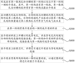
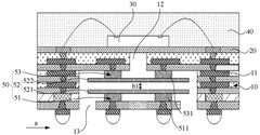
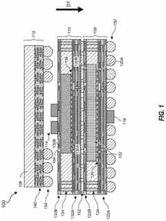
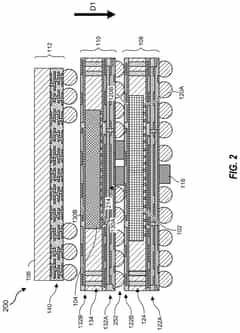
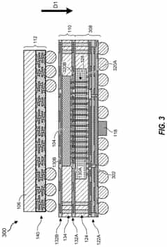
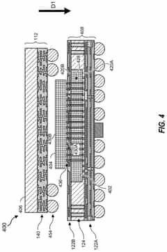
Semiconductor packaging structure and preparation method thereof
PatentActiveCN118431177B
Innovation
- A semiconductor packaging structure is designed, including a wiring structure with conductive lines, a dielectric layer, a chip and a cooling structure. The cooling structure is electrically connected to the conductive lines. After being energized, it vibrates to form an airflow pressure difference and communicates with the outside air through the first heat dissipation hole. An airflow pressure difference is formed to improve heat dissipation performance, and the chip is packaged through the dielectric layer and plastic sealing layer to avoid external power supply interference.
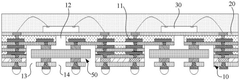
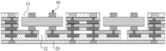
3D chiplet integration using fan-out wafer-level packaging
PatentPendingUS20240274587A1
Innovation
- The use of fan-out wafer-level packaging and three-dimensional packaging techniques for combining semiconductor chips and embedded memory in configurations such as face-to-back, back-to-back, and face-to-face orientations, enabling direct connections between chiplets and reducing assembly package sizes and manufacturing complexity.
Energy Efficiency Metrics and Benchmarking
Establishing standardized energy efficiency metrics for chiplet integration is crucial for meaningful performance comparisons across different semiconductor designs. The industry currently employs several key metrics to evaluate chiplet-based systems' energy efficiency. Power Usage Effectiveness (PUE) measures the ratio between total power consumed and power delivered to computing components, providing insights into overhead energy costs. Energy Delay Product (EDP) combines performance and energy consumption metrics, offering a more comprehensive efficiency assessment by multiplying energy consumption by execution time.
Performance per Watt (PPW) represents computational output relative to power input, serving as a fundamental efficiency indicator particularly valuable for data center applications where operating costs are directly tied to energy consumption. Thermal Design Power (TDP) establishes maximum heat generation thresholds, critical for cooling system design and thermal management strategies in chiplet architectures where heat dissipation presents unique challenges due to integration density.
Benchmarking methodologies have evolved to address chiplet-specific considerations. SPEC Power benchmarks evaluate server efficiency under various workloads, while MLPerf measures machine learning workload efficiency across different hardware configurations. The Green500 list ranks supercomputers by FLOPS per watt, providing valuable comparative data for high-performance computing applications utilizing chiplet technology.
Industry-specific benchmarks are emerging to address unique chiplet integration challenges. These include die-to-die (D2D) interface efficiency metrics measuring communication energy per bit transferred between chiplets, and system-level benchmarks evaluating overall platform efficiency including memory hierarchies and interconnect technologies. The Chiplet Energy Efficiency Factor (CEEF) has been proposed as a composite metric accounting for both computational efficiency and communication overhead between chiplets.
Standardization efforts are underway through organizations like JEDEC and the Open Compute Project to establish uniform testing methodologies. These initiatives aim to create consistent measurement protocols enabling fair comparisons between different chiplet integration approaches. The development of application-specific benchmarks further enhances evaluation accuracy by simulating real-world workloads rather than synthetic tests, providing more relevant efficiency data for specific use cases.
Supply Chain Implications for Chiplet Adoption
The adoption of chiplet technology is fundamentally reshaping semiconductor supply chains, creating both opportunities and challenges for industry participants. Traditional monolithic chip production relies on vertically integrated supply chains where a single manufacturer controls most aspects of production. In contrast, chiplet architecture enables a more modular approach, allowing specialized suppliers to focus on specific components that can be integrated later through advanced packaging technologies.
This shift towards disaggregation creates new entry points for specialized manufacturers who can now participate in the semiconductor value chain without mastering the entire production process. Small and medium enterprises can focus on designing specialized chiplets for specific functions, potentially democratizing aspects of semiconductor innovation that were previously accessible only to industry giants.
The geographical distribution of the supply chain is also evolving with chiplet adoption. While traditional semiconductor manufacturing has been concentrated in East Asia, chiplet technology may enable regional manufacturing clusters to develop around specific types of chiplets or packaging technologies. This could partially address concerns about supply chain concentration and geopolitical vulnerabilities that have become prominent in recent years.
Inventory management strategies must adapt to accommodate chiplet-based production models. Companies need to develop new forecasting methods that account for the interchangeability of chiplets across different end products, potentially reducing overall inventory requirements while increasing flexibility in production planning.
Quality control presents unique challenges in a chiplet ecosystem. Testing protocols must evolve to verify not only individual chiplet functionality but also integration compatibility. This necessitates new standards for interoperability and testing methodologies across the supply chain, requiring unprecedented collaboration among previously competitive entities.
The transition to chiplet-based production also impacts logistics networks. While individual chiplets may be smaller and easier to transport than complete systems-on-chip, the increased complexity of managing multiple component sources requires more sophisticated supply chain coordination systems. Advanced tracking technologies and digital supply chain platforms are becoming essential infrastructure for chiplet-based manufacturing ecosystems.
Ultimately, chiplet adoption may lead to more resilient semiconductor supply chains through diversification of suppliers and manufacturing locations, but this transition requires significant investment in new coordination mechanisms, standards development, and testing protocols to realize its full potential.
Unlock deeper insights with Patsnap Eureka Quick Research — get a full tech report to explore trends and direct your research. Try now!
Generate Your Research Report Instantly with AI Agent
Supercharge your innovation with Patsnap Eureka AI Agent Platform!