CO₂ Capture Sorbent Standards in the Electronics Industry
SEP 28, 20259 MIN READ
Generate Your Research Report Instantly with AI Agent
Patsnap Eureka helps you evaluate technical feasibility & market potential.
CO₂ Capture Technology Evolution and Objectives
Carbon dioxide capture technology has evolved significantly over the past several decades, transitioning from theoretical concepts to practical applications across various industries. The electronics manufacturing sector, with its precision requirements and clean room environments, presents unique challenges and opportunities for CO₂ capture implementation. Initially developed for large-scale industrial applications such as power plants and chemical processing facilities, CO₂ capture technologies have undergone substantial refinement to address the specialized needs of electronics fabrication processes.
The historical trajectory of CO₂ sorbent development reveals a progression from basic chemical absorption methods using aqueous amines to more sophisticated solid sorbents with enhanced selectivity and regeneration capabilities. Early approaches in the 1990s focused primarily on post-combustion capture for large emission sources, with limited consideration for the high-purity requirements essential in electronics manufacturing environments.
By the early 2000s, research began exploring specialized sorbent materials with improved CO₂ selectivity and reduced energy penalties during regeneration. This period marked the emergence of metal-organic frameworks (MOFs), zeolites, and functionalized porous materials specifically engineered for targeted CO₂ capture applications. These advances laid the groundwork for the development of sorbent standards applicable to the electronics industry's stringent requirements.
The primary technical objectives for CO₂ capture sorbents in electronics manufacturing center on achieving high capture efficiency while maintaining ultra-low contamination profiles. Unlike conventional industrial applications, electronics fabrication demands sorbents that release minimal particulates, introduce no metallic contaminants, and generate no outgassing that might compromise semiconductor or display manufacturing processes. Additionally, these sorbents must function effectively at the relatively low CO₂ concentrations typically found in cleanroom environments.
Current technological goals include developing standardized testing protocols for evaluating sorbent performance specifically for electronics applications. These standards aim to quantify parameters such as capture capacity, selectivity over other gases, regeneration efficiency, particulate generation, outgassing profiles, and long-term stability under cleanroom operating conditions. The establishment of these standards represents a critical step toward enabling widespread adoption of CO₂ capture technologies within the electronics manufacturing sector.
Looking forward, the technology roadmap emphasizes the development of next-generation sorbents that combine high performance with compatibility with existing fabrication infrastructure. This includes exploring novel materials that can be integrated into current HVAC and gas purification systems without requiring extensive facility modifications or introducing new contamination risks to sensitive manufacturing processes.
Electronics Industry Demand for CO₂ Capture Solutions
The electronics industry is experiencing a significant shift towards sustainable manufacturing practices, with carbon dioxide (CO₂) emissions reduction becoming a critical focus area. This transition is driven by multiple factors, including increasingly stringent environmental regulations, corporate sustainability commitments, and growing consumer demand for environmentally responsible products. As semiconductor and electronics manufacturing processes are energy-intensive and generate substantial carbon emissions, the industry faces mounting pressure to implement effective carbon capture solutions.
Market research indicates that the global electronics sector accounts for approximately 2-3% of global carbon emissions, with projections showing this figure could rise significantly without intervention. Major electronics manufacturers have publicly committed to achieving carbon neutrality within the next decade, creating immediate demand for scalable CO₂ capture technologies that can be integrated into existing manufacturing facilities.
The demand is particularly acute in semiconductor fabrication plants, where ultra-pure environments are required. These facilities need specialized CO₂ capture solutions that can operate without introducing contaminants into the manufacturing process. Traditional carbon capture technologies often involve chemicals or processes incompatible with the stringent cleanliness requirements of chip manufacturing.
Consumer electronics companies are increasingly incorporating carbon footprint metrics into their product lifecycle assessments, driving demand throughout the supply chain for components manufactured using low-carbon processes. This market pressure has created a competitive advantage for suppliers who can demonstrate reduced carbon intensity in their manufacturing operations.
Regional variations in demand exist, with electronics manufacturers in Europe facing more immediate regulatory pressure compared to those in other regions. However, global supply chain considerations mean that even manufacturers based in regions with less stringent regulations are seeking carbon capture solutions to maintain access to international markets.
The electronics industry presents unique technical requirements for CO₂ capture solutions. These include the need for systems that can operate in cleanroom environments, compatibility with existing HVAC systems, minimal space requirements due to the high cost of manufacturing floor space, and energy efficiency to avoid offsetting carbon reduction gains with increased energy consumption.
Financial analyses suggest that electronics manufacturers are willing to invest in carbon capture technologies with return-on-investment periods of 3-5 years, particularly if these solutions help them avoid carbon taxes or qualify for green manufacturing incentives. This represents a significant market opportunity for developers of specialized CO₂ capture sorbents tailored to the unique requirements of electronics manufacturing.
Global Status and Barriers in CO₂ Sorbent Development
The global landscape of CO₂ capture sorbent development presents a complex picture of progress and challenges. Currently, the most advanced CO₂ sorbent technologies include amine-based solid sorbents, metal-organic frameworks (MOFs), zeolites, and activated carbon materials. These technologies have demonstrated varying degrees of CO₂ capture efficiency, with some laboratory-scale systems achieving over 90% capture rates under controlled conditions.
In North America and Europe, significant research infrastructure and funding have accelerated sorbent development, with particular emphasis on materials suitable for industrial applications including electronics manufacturing. Japan and South Korea lead the Asia-Pacific region in specialized sorbent development for high-purity applications critical to semiconductor production environments.
Despite these advancements, several critical barriers impede widespread implementation of CO₂ capture sorbents in the electronics industry. Technical challenges include insufficient selectivity for CO₂ in mixed gas streams typical of cleanroom environments, degradation of sorbent materials after multiple regeneration cycles, and energy-intensive regeneration processes that contradict sustainability goals.
Economic barriers represent another significant obstacle. Current production costs for high-performance sorbents remain prohibitively high for large-scale deployment, with estimates suggesting prices between $200-500 per kilogram for specialized electronics-grade materials. The capital investment required for integration of capture systems into existing manufacturing facilities further complicates adoption.
Regulatory inconsistencies across global markets create additional complications. The absence of unified international standards for CO₂ capture sorbents in electronics manufacturing has resulted in fragmented approaches to certification and implementation. This regulatory uncertainty discourages investment in technology development and commercialization pathways.
Infrastructure limitations also present challenges. Many electronics manufacturing facilities lack the physical space and utility connections necessary for retrofitting carbon capture systems. The integration of capture technologies with existing cleanroom environments poses unique engineering challenges related to contamination control and process stability.
Knowledge gaps further hinder progress, particularly regarding long-term performance of sorbents under real-world manufacturing conditions. Limited data exists on how semiconductor process chemicals interact with various sorbent materials over extended operational periods. Additionally, the specialized nature of electronics manufacturing creates unique requirements for sorbent purity and performance that have not been adequately addressed by broader carbon capture research.
Current CO₂ Sorbent Standards and Implementation
01 Adsorbent materials for CO₂ capture
Various materials can be used as adsorbents for CO₂ capture, including zeolites, metal-organic frameworks (MOFs), activated carbons, and amine-functionalized materials. These materials have high surface areas and specific binding sites for CO₂ molecules, allowing for efficient capture. The performance of these adsorbents is evaluated based on their CO₂ adsorption capacity, selectivity, and regeneration efficiency under different operating conditions.- Amine-based CO₂ capture sorbents: Amine-based materials are widely used as CO₂ capture sorbents due to their high selectivity and capacity. These sorbents typically consist of amine functional groups supported on porous materials such as silica or activated carbon. The amine groups react with CO₂ through chemisorption, forming carbamates or bicarbonates. Standards for these sorbents focus on amine loading, CO₂ capture capacity, regeneration energy requirements, and stability over multiple adsorption-desorption cycles.
- Metal-organic frameworks (MOFs) for CO₂ capture: Metal-organic frameworks represent an advanced class of CO₂ capture sorbents with highly tunable pore structures and surface chemistry. These crystalline materials consist of metal ions or clusters coordinated to organic ligands, creating porous structures with exceptionally high surface areas. Standards for MOF-based sorbents address crystallinity, pore volume, surface area, hydrothermal stability, and CO₂ selectivity over other gases. The performance metrics include adsorption capacity under various temperature and pressure conditions, as well as structural integrity after multiple adsorption-desorption cycles.
- Zeolite and molecular sieve standards for CO₂ capture: Zeolites and molecular sieves are aluminosilicate materials with well-defined pore structures that can selectively adsorb CO₂. Standards for these materials focus on Si/Al ratio, pore size distribution, cation content, and hydrophobicity. Performance standards include CO₂ adsorption capacity at different partial pressures, selectivity over nitrogen and water vapor, and regeneration temperature requirements. The durability standards address thermal stability, resistance to steam, and performance retention after exposure to contaminants typically found in flue gas streams.
- Carbon-based CO₂ capture sorbents: Carbon-based materials, including activated carbon, carbon nanotubes, and graphene derivatives, serve as effective CO₂ capture sorbents. Standards for these materials address surface area, pore size distribution, surface functionality, and preparation methods. Performance metrics include CO₂ adsorption capacity under various conditions, selectivity, regeneration energy, and cycle stability. The standards also cover modification techniques such as nitrogen doping, metal impregnation, and oxidative treatments that enhance CO₂ capture performance. Environmental and economic considerations include raw material sourcing, production energy requirements, and end-of-life disposal.
- Testing protocols and performance metrics for CO₂ capture sorbents: Standardized testing protocols are essential for evaluating and comparing CO₂ capture sorbents. These standards define experimental conditions including temperature, pressure, gas composition, flow rates, and humidity levels. Key performance metrics include equilibrium adsorption capacity, adsorption kinetics, working capacity, selectivity, and regenerability. The standards also address accelerated aging tests to predict long-term stability, mechanical strength measurements, and attrition resistance. Economic evaluation metrics include cost per ton of CO₂ captured, energy penalty, and overall process efficiency. Reporting standards ensure data transparency and reproducibility across different research groups and industrial applications.
02 Testing methods for CO₂ sorbent performance
Standardized testing methods are essential for evaluating the performance of CO₂ capture sorbents. These methods include breakthrough tests, temperature-programmed desorption, pressure swing adsorption cycles, and accelerated aging tests. Testing protocols typically measure parameters such as adsorption capacity, selectivity, kinetics, mechanical stability, and performance degradation over multiple cycles under conditions that simulate real-world applications.Expand Specific Solutions03 Regeneration and cyclic stability standards
Standards for CO₂ capture sorbents include specifications for regeneration efficiency and cyclic stability. These standards define acceptable levels of performance degradation over multiple adsorption-desorption cycles, energy requirements for regeneration, and methods to evaluate sorbent lifetime. Regeneration can be achieved through temperature swing, pressure swing, or vacuum swing processes, with each method having specific performance metrics and energy consumption benchmarks.Expand Specific Solutions04 Environmental and safety standards for CO₂ sorbents
Environmental and safety standards for CO₂ capture sorbents address toxicity, environmental impact, and handling requirements. These standards specify acceptable levels of emissions during production and use, biodegradability of materials, and safety protocols for handling potentially hazardous components. Compliance with these standards ensures that CO₂ capture technologies do not create secondary environmental problems while solving carbon emission issues.Expand Specific Solutions05 Performance metrics and quality control standards
Quality control standards for CO₂ capture sorbents establish performance metrics and manufacturing consistency requirements. These standards define acceptable ranges for particle size distribution, mechanical strength, moisture sensitivity, and chemical composition. They also specify methods for batch-to-batch quality control testing and certification procedures to ensure that commercial sorbents meet minimum performance requirements for industrial applications.Expand Specific Solutions
Leading Companies in CO₂ Capture Sorbent Market
The CO₂ capture sorbent market in the electronics industry is in its growth phase, with increasing adoption driven by sustainability regulations. The competitive landscape features diverse players across the value chain, including major energy corporations (Saudi Aramco, Shell, CNOOC), research institutions (Dalian University of Technology, Dalian Institute of Chemical Physics), and specialized technology providers (Skyre, GTI Energy). Market size is expanding as electronics manufacturers seek to reduce carbon footprints. Technology maturity varies significantly, with established players like Schlumberger and Sharp developing proprietary solutions, while academic institutions (University of California, Shandong University) focus on fundamental research. Collaboration between industry and academia is accelerating commercialization of novel sorbent technologies optimized for electronics manufacturing environments.
Saudi Arabian Oil Co.
Technical Solution: Saudi Arabian Oil Co. (Saudi Aramco) has developed advanced Metal-Organic Framework (MOF) based sorbents specifically designed for CO₂ capture in electronics manufacturing facilities. Their proprietary MOF materials feature exceptionally high surface areas (>2000 m²/g) and tailored pore structures that enable selective adsorption of CO₂ even at the low concentrations typical in cleanroom environments. The company has integrated these sorbents into modular capture units that can be retrofitted to existing semiconductor fabrication facilities with minimal disruption to operations. Their system incorporates a novel temperature-swing adsorption process that achieves over 90% CO₂ recovery while consuming approximately 40% less energy than conventional amine-based systems. Saudi Aramco has also developed specialized regeneration protocols that maintain sorbent performance over hundreds of cycles, addressing a key challenge in industrial implementation.
Strengths: High selectivity for CO₂ even at low concentrations; energy-efficient regeneration process; modular design allows easy integration with existing facilities; proven durability over multiple cycles. Weaknesses: Higher initial capital costs compared to conventional systems; requires specialized expertise for maintenance; performance may degrade in high-humidity environments.
Dalian Institute of Chemical Physics of CAS
Technical Solution: Dalian Institute of Chemical Physics (DICP) has pioneered innovative ionic liquid-based CO₂ capture sorbents specifically engineered for electronics manufacturing environments. Their technology utilizes task-specific ionic liquids (TSILs) with functionalized anions that demonstrate exceptional CO₂ selectivity (>95%) even in the presence of other process gases common in semiconductor fabrication. DICP's sorbent formulations maintain stable performance under the ultra-clean conditions required in electronics manufacturing, with contaminant release rates below 1 ppb. Their system incorporates a continuous flow absorption-desorption cycle that operates at near-ambient pressures, reducing energy requirements by approximately 35% compared to conventional pressure-swing systems. The institute has also developed specialized coating techniques that maximize the active surface area of the ionic liquids when applied to structured supports, achieving CO₂ capture rates of 0.5-0.7 mol CO₂/mol ionic liquid under typical cleanroom conditions.
Strengths: Exceptional selectivity for CO₂; minimal contamination risk suitable for cleanroom environments; operates at near-ambient pressure conditions; relatively low energy requirements for regeneration. Weaknesses: Higher production costs compared to conventional sorbents; potential for performance degradation over extended operation periods; limited large-scale implementation experience in industrial settings.
Key Patents and Research in CO₂ Capture Materials
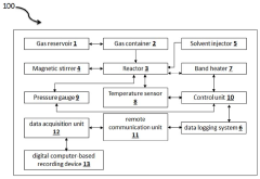
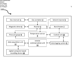
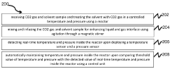
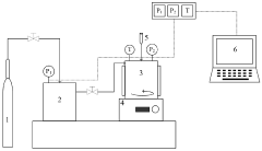
A system and method for capturing carbon dioxide (CO2)
PatentActiveIN202241058443A
Innovation
- A system and method utilizing a reactor with a solvent injector, magnetic stirrer, temperature sensor, and pressure gauge to treat CO2 gas with a solvent in controlled conditions, enhancing the liquid-gas interface and employing deep eutectic solvents (DES) as an alternative to conventional amine-based technologies, aiming to reduce energy consumption and improve CO2 absorption capacity.
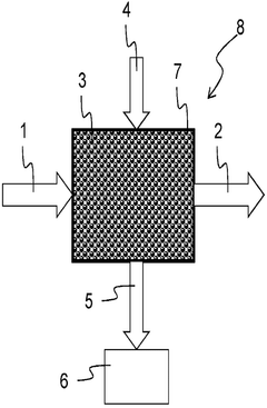
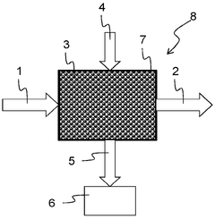
Co2 adsorption system and method for co2 adsorption using humidity stable polystyrene-divinylbenzene amine functionalized polymeric adsorbents
PatentPendingCA3240579A1
Innovation
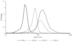
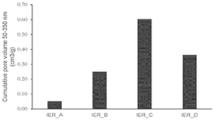
- Development of sorbent materials with specific surface areas between 10-25 m2/g and cumulative pore volumes in the range of 50-350 nm, which exhibit stable carbon dioxide adsorption behavior independent of humidity levels, utilizing cross-linked polystyrene-divinylbenzene (DVB) with amino functionalization, enabling effective CO2 capture across a wide range of relative humidity conditions.
Environmental Impact Assessment of CO₂ Capture Solutions
The environmental impact of CO₂ capture solutions in the electronics industry extends far beyond the immediate reduction of greenhouse gas emissions. When evaluating these technologies, a comprehensive life cycle assessment (LCA) approach is essential to understand their true environmental footprint. Current CO₂ capture sorbents used in electronics manufacturing facilities demonstrate varying degrees of environmental performance across multiple impact categories.
Primary environmental considerations include the energy intensity of sorbent regeneration processes, which can significantly offset carbon reduction benefits if powered by fossil fuel sources. Research indicates that amine-based sorbents, while effective for CO₂ capture, often require substantial thermal energy for regeneration, potentially creating a counterproductive environmental trade-off unless renewable energy sources are employed.
Water consumption represents another critical environmental factor, particularly in semiconductor manufacturing regions already experiencing water stress. Metal-organic frameworks (MOFs) and certain zeolite-based sorbents demonstrate more favorable water efficiency profiles compared to traditional wet scrubbing technologies, reducing the overall water footprint by approximately 30-45% according to recent industry benchmarking studies.
The production and disposal of spent sorbent materials introduce additional environmental considerations. Solid sorbents containing heavy metals or toxic compounds can create hazardous waste management challenges, while the mining and processing of raw materials for sorbent production may contribute to habitat destruction and biodiversity loss in source regions. Recent innovations in bio-based sorbents derived from waste biomass show promise in reducing these upstream environmental impacts.
Land use implications vary significantly between capture technologies. Direct air capture (DAC) systems deployed at electronics manufacturing facilities require substantial space allocation, potentially competing with other land uses in densely developed industrial parks. In contrast, point-source capture systems integrated directly into production equipment offer more space-efficient solutions with minimal additional land requirements.
Cross-media pollution effects must also be considered, as some capture technologies may reduce carbon emissions while simultaneously increasing other pollutants. For instance, certain amine-based systems have been documented to increase ammonia emissions and potentially contribute to particulate matter formation in surrounding areas.
The electronics industry's adoption of standardized environmental impact metrics for CO₂ capture solutions would enable more transparent comparison between competing technologies. Current industry leaders are increasingly implementing ISO 14040/14044-compliant assessment methodologies to quantify impacts across multiple environmental dimensions, moving beyond simple carbon accounting to more holistic sustainability evaluation frameworks.
Regulatory Framework for Carbon Capture in Electronics
The regulatory landscape for carbon capture technologies in the electronics industry is evolving rapidly as governments worldwide implement stricter environmental policies. The European Union leads with its European Green Deal, which mandates carbon neutrality by 2050 and includes specific provisions for electronics manufacturing. The EU's Emissions Trading System (ETS) has been expanded to cover semiconductor production facilities, creating financial incentives for implementing carbon capture technologies.
In the United States, the EPA has established the Clean Air Act regulations that increasingly target electronics manufacturing emissions. The 45Q tax credit provides significant financial benefits for companies implementing carbon capture, utilization, and storage (CCUS) technologies, offering up to $50 per metric ton of CO₂ captured. Additionally, the CHIPS and Science Act of 2022 includes provisions for environmental sustainability in semiconductor manufacturing.
Asian countries, particularly Japan, South Korea, and Taiwan, have developed specialized regulatory frameworks addressing the unique challenges of electronics manufacturing. Taiwan's Greenhouse Gas Reduction and Management Act specifically targets the semiconductor industry, requiring annual emissions reporting and reduction targets. South Korea's K-ETS (Korea Emissions Trading Scheme) includes electronics manufacturers as key participants.
International standards organizations play a crucial role in harmonizing regulatory approaches. The ISO 14000 series provides environmental management standards applicable to electronics manufacturing, while the newly developed ISO/TC 265 focuses specifically on carbon capture technologies. The International Electronics Manufacturing Initiative (iNEMI) has established industry-specific guidelines for measuring and reporting carbon emissions in electronics production.
Compliance verification mechanisms are becoming increasingly sophisticated. Third-party verification of carbon capture efficiency is now mandatory in many jurisdictions, with specific requirements for measurement accuracy and reporting frequency. The electronics industry faces unique challenges in this regard, as CO₂ emissions from semiconductor manufacturing often contain specialized process gases that require custom capture solutions.
Looking forward, regulatory trends indicate increasing stringency and harmonization. The proposed Carbon Border Adjustment Mechanism (CBAM) in the EU will likely impact global electronics supply chains by imposing carbon-related tariffs. Industry stakeholders anticipate the development of specialized standards for CO₂ sorbent materials used in electronics manufacturing environments, addressing concerns about contamination risks and compatibility with cleanroom environments.
Unlock deeper insights with Patsnap Eureka Quick Research — get a full tech report to explore trends and direct your research. Try now!
Generate Your Research Report Instantly with AI Agent
Supercharge your innovation with Patsnap Eureka AI Agent Platform!