

Comparing Chiplet Integration Techniques in Semiconductor Processes
OCT 15, 20259 MIN READ
Generate Your Research Report Instantly with AI Agent
PatSnap Eureka helps you evaluate technical feasibility & market potential.
Chiplet Technology Evolution and Objectives
The evolution of semiconductor technology has been marked by continuous miniaturization following Moore's Law for decades. However, as traditional scaling approaches physical limits, chiplet technology has emerged as a revolutionary paradigm shift in semiconductor design and manufacturing. This architectural innovation enables the disaggregation of monolithic systems-on-chip (SoCs) into smaller functional blocks called chiplets, which can be manufactured separately and then integrated into a single package.
The concept of chiplet technology originated in the early 2000s but gained significant momentum around 2015-2017 when major semiconductor companies began facing yield challenges with advanced process nodes. The fundamental principle involves breaking down complex designs into smaller, more manageable die pieces that can be manufactured with higher yields and then assembled using advanced packaging technologies.
From 2017 to 2020, the industry witnessed the first commercial implementations of chiplet-based products, with AMD's Ryzen processors utilizing their Infinity Fabric interconnect technology to combine multiple CPU dies. Intel followed with their Embedded Multi-die Interconnect Bridge (EMIB) and Foveros technologies, while TSMC developed their Integrated Fan-Out (InFO) and System on Integrated Chips (SoIC) solutions.
The technological trajectory has been characterized by continuous improvements in die-to-die interconnect bandwidth, power efficiency, and manufacturing processes. The development of industry standards like Universal Chiplet Interconnect Express (UCIe) in 2022 marked a significant milestone toward enabling interoperability between chiplets from different vendors, potentially creating a more diverse ecosystem.
The primary objectives of chiplet technology development include overcoming the limitations of monolithic integration, improving manufacturing yields, enabling heterogeneous integration of components manufactured at different process nodes, and reducing development costs and time-to-market for complex semiconductor products.
Current research focuses on advancing interconnect technologies to minimize the performance gap between chiplet-based designs and monolithic implementations. This includes reducing the energy cost of data movement between chiplets, increasing bandwidth density, and developing more sophisticated packaging solutions that can accommodate greater numbers of chiplets with precise alignment requirements.
Looking forward, the industry aims to establish a robust chiplet ecosystem with standardized interfaces, design methodologies, and testing protocols. The ultimate goal is to enable a modular approach to semiconductor design where pre-validated chiplets from various vendors can be efficiently integrated, similar to how printed circuit boards combine discrete components today, but at a much finer granularity and higher performance level.
Market Demand Analysis for Chiplet Integration
The chiplet integration market is experiencing unprecedented growth, driven by the semiconductor industry's need to overcome the limitations of traditional monolithic chip designs. As Moore's Law faces increasing physical and economic constraints, chiplet technology has emerged as a viable solution for continued performance scaling. Market research indicates that the global chiplet market is projected to grow at a compound annual growth rate of 40% from 2023 to 2030, reaching significant market valuation by the end of the decade.
This rapid market expansion is primarily fueled by data centers and high-performance computing applications, which demand ever-increasing computational power while maintaining energy efficiency. These sectors currently represent approximately 45% of the total chiplet market demand, with telecommunications and consumer electronics following closely behind.
The demand for chiplet integration is further accelerated by the rising costs of advanced semiconductor manufacturing processes. As process nodes shrink below 5nm, the development and production costs have become prohibitively expensive, even for major industry players. Chiplet architecture offers a cost-effective alternative by allowing manufacturers to combine mature process nodes with cutting-edge technology, optimizing both performance and production expenses.
Industry surveys reveal that 78% of semiconductor companies are actively investing in chiplet technology development, recognizing it as a strategic priority. This trend is particularly evident in regions with established semiconductor ecosystems, such as North America, East Asia, and Europe, where significant research and development resources are being allocated to chiplet integration techniques.
From a supply chain perspective, chiplet technology addresses critical vulnerabilities exposed during recent global disruptions. By enabling more modular and flexible manufacturing approaches, chiplet integration reduces dependency on single-source components and allows for greater geographical distribution of production capabilities.
The market is also witnessing increased demand for standardization in chiplet interfaces and packaging technologies. The Universal Chiplet Interconnect Express (UCIe) consortium, formed by major industry players, demonstrates the industry's recognition of interoperability as a key market driver. Standardization efforts are expected to expand the chiplet ecosystem and accelerate adoption across various market segments.
Customer requirements are evolving toward more customized computing solutions, particularly in emerging fields such as artificial intelligence, autonomous vehicles, and edge computing. Chiplet architecture enables greater design flexibility and faster time-to-market for specialized applications, meeting these evolving market demands more effectively than traditional monolithic approaches.
Current Challenges in Chiplet Integration Techniques
Despite significant advancements in chiplet integration technologies, several critical challenges continue to impede the widespread adoption and optimization of these approaches. The primary obstacle remains the interconnect bottleneck, where achieving high-bandwidth, low-latency, and energy-efficient connections between chiplets presents significant technical difficulties. Current die-to-die interfaces struggle to match the performance metrics of monolithic designs, particularly in terms of bandwidth density and power efficiency.
Manufacturing challenges also persist, especially in achieving precise alignment during the assembly process. The micron-level accuracy required for advanced packaging techniques such as silicon interposers and direct bonding demands specialized equipment and processes that increase production complexity and costs. Thermal management represents another significant hurdle, as heat dissipation becomes more complex in multi-chiplet designs where thermal paths are interrupted by interfaces between components.
Testing methodologies for chiplet-based systems remain underdeveloped compared to traditional monolithic approaches. Known-good-die testing before integration is essential but challenging to implement comprehensively, while post-integration testing faces limitations in fault isolation and diagnosis. This testing gap increases manufacturing risks and potentially impacts yield rates.
Standardization issues further complicate the chiplet ecosystem. The lack of universal interfaces and protocols forces designers to create custom solutions for each implementation, hindering interoperability between chiplets from different vendors. Industry initiatives like UCIe (Universal Chiplet Interconnect Express) are emerging but have yet to achieve widespread adoption or cover all necessary aspects of chiplet integration.
Design tools and methodologies present additional challenges. EDA tools optimized for traditional monolithic designs often lack comprehensive support for chiplet-based architectures, particularly in modeling the complex interactions between multiple dies. System-level optimization across chiplets requires sophisticated co-design approaches that consider physical, electrical, and thermal interactions simultaneously.
Supply chain complexity increases substantially with chiplet designs, as manufacturers must coordinate multiple fabrication processes, potentially across different foundries and packaging facilities. This coordination introduces logistical challenges and potential vulnerabilities in the production pipeline.
Finally, cost considerations remain paramount. While chiplet approaches theoretically offer cost advantages through improved yield and process optimization, the additional expenses associated with advanced packaging, testing, and design complexity can offset these benefits. The economic equation varies significantly based on production volume, design complexity, and performance requirements, making the business case for chiplet adoption highly context-dependent.
Mainstream Chiplet Integration Solutions
01 Advanced Interconnect Technologies for Chiplet Integration
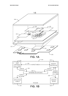
Various interconnect technologies are employed to facilitate communication between chiplets in multi-die systems. These include high-bandwidth die-to-die interfaces, through-silicon vias (TSVs), and advanced packaging techniques that enable high-speed data transfer with minimal latency. These interconnect solutions are crucial for maintaining performance while distributing functionality across multiple chiplets, allowing for modular system design and improved yield.- Advanced Interconnect Technologies for Chiplet Integration: Various interconnect technologies are employed to facilitate communication between chiplets in multi-die systems. These include high-bandwidth interfaces, through-silicon vias (TSVs), and advanced packaging techniques that enable high-speed data transfer between different chiplets. These interconnect solutions are designed to minimize latency and power consumption while maximizing bandwidth, which is crucial for maintaining system performance in disaggregated chip architectures.
- Thermal Management Solutions for Chiplet Designs: Thermal management is critical in chiplet-based systems due to the high power density and potential hotspots at interconnect points. Innovative cooling solutions include integrated heat spreaders, thermal interface materials specifically designed for chiplet architectures, and advanced cooling techniques that address the unique thermal challenges of multi-die packages. These solutions help maintain optimal operating temperatures across all chiplets, ensuring reliability and consistent performance.
- Power Distribution and Management in Chiplet Systems: Effective power distribution is essential in chiplet-based designs to ensure stable operation across multiple dies. This includes advanced power delivery networks, integrated voltage regulators, and power management techniques that can dynamically adjust power allocation based on workload requirements. These systems must address the challenges of delivering clean power across chiplet boundaries while minimizing power loss and electromagnetic interference between components.
- Heterogeneous Integration of Chiplets: Heterogeneous integration involves combining chiplets manufactured using different process technologies or containing different functional blocks. This approach allows for optimizing each chiplet for its specific function while maintaining system-level integration. Techniques include die-to-die bonding methods, interposer technologies, and bridge structures that enable chiplets with varying characteristics to work together seamlessly, maximizing overall system performance while potentially reducing costs.
- Testing and Yield Improvement for Chiplet-Based Systems: Testing methodologies specific to chiplet architectures are essential for ensuring reliability and improving manufacturing yield. These include known-good-die testing before integration, built-in self-test capabilities for interconnects, and post-assembly validation techniques. Advanced testing approaches help identify defects at various stages of the manufacturing process, allowing for better yield management and potentially enabling the use of chiplets that would otherwise be discarded in monolithic designs.
02 Thermal Management Solutions for Chiplet Architectures
Effective thermal management is essential in chiplet-based designs due to the high power density and potential hotspots at interconnect points. Techniques include integrated heat spreaders, thermal interface materials specifically designed for multi-die packages, and advanced cooling solutions that address the unique thermal challenges of chiplet architectures. These solutions help maintain optimal operating temperatures across all chiplets, ensuring reliability and consistent performance.Expand Specific Solutions03 Power Distribution and Management for Multi-Chiplet Systems
Efficient power delivery is critical in chiplet-based designs to ensure stable operation across multiple dies. Techniques include integrated voltage regulators, advanced power distribution networks, and power management ICs specifically designed for heterogeneous integration. These solutions address the challenges of delivering appropriate power to different chiplets with varying voltage requirements while minimizing power loss and electromagnetic interference between components.Expand Specific Solutions04 Heterogeneous Integration of Chiplets
Heterogeneous integration involves combining chiplets manufactured using different process technologies or having different functionalities into a single package. This approach allows for optimizing each chiplet for its specific function while maintaining system-level integration. Techniques include advanced packaging platforms, interposer technologies, and bridge structures that enable chiplets from different manufacturers or process nodes to work together seamlessly, maximizing performance while controlling costs.Expand Specific Solutions05 Testing and Yield Improvement Strategies for Chiplet-Based Systems
Testing methodologies specific to chiplet architectures are essential for ensuring reliability and improving yield. These include known-good-die testing before integration, built-in self-test capabilities for interconnects, and post-assembly validation techniques. Advanced testing strategies help identify defects early in the manufacturing process, allowing for the replacement of faulty chiplets rather than discarding entire systems, thereby improving overall yield and reducing costs.Expand Specific Solutions
Key Semiconductor Players in Chiplet Ecosystem
The chiplet integration market is currently in a growth phase, with major players advancing different techniques to overcome traditional semiconductor scaling limitations. The market size is expanding rapidly as chiplet technology enables cost-effective performance improvements beyond Moore's Law constraints. Leading semiconductor manufacturers like TSMC, Intel, and AMD are at the forefront, with TSMC's advanced packaging solutions gaining significant traction. IBM and Micron are contributing innovative memory integration approaches, while research institutions like Imec and ETRI are developing next-generation interconnect technologies. Companies like ASE and Applied Materials are providing critical packaging infrastructure. The technology maturity varies across integration methods, with 2.5D interposers being more established while true 3D integration remains emerging, creating a competitive landscape where different approaches are competing for market dominance.
International Business Machines Corp.
Technical Solution: IBM has pioneered several chiplet integration technologies, with their Silicon Carrier Packaging Technology (SCPT) representing an early implementation of silicon interposers for high-bandwidth chip-to-chip connections. Their current approach centers around their Direct Bonded Heterogeneous Integration (DBHI) technology, which enables face-to-face bonding of chiplets with micron-scale interconnect pitches. IBM's Silicon Space Technology (SST) further extends their capabilities by implementing through-silicon vias (TSVs) for vertical integration of chiplets. Their most advanced implementation is seen in the POWER10 processor, which uses a modular design with separate core and I/O chiplets. IBM has also developed specialized cooling solutions for high-density chiplet implementations, including their Direct Jet Impingement technology that targets hotspots in multi-chip modules. Their research collaboration with Tokyo Electron has yielded advances in hybrid bonding techniques that achieve sub-3μm interconnect pitches between stacked dies[7][8]. IBM's approach emphasizes precision alignment technologies that enable die-to-die bonding with less than 0.2μm misalignment, critical for their high-density interconnect strategies.
Strengths: IBM's long history in advanced packaging provides deep expertise in thermal management of multi-chip modules. Their research-driven approach has yielded industry-leading interconnect densities. Their vertical integration capabilities allow for optimized system-level designs. Weaknesses: Their technologies often require specialized manufacturing equipment, limiting widespread adoption. Their focus on high-performance computing applications may make their approaches less cost-effective for consumer applications. Their chiplet ecosystem is less developed than some competitors.
Taiwan Semiconductor Manufacturing Co., Ltd.
Technical Solution: TSMC has developed several advanced chiplet integration technologies, with their Chip-on-Wafer-on-Substrate (CoWoS) platform serving as their flagship offering. CoWoS uses silicon interposers with through-silicon vias (TSVs) to provide high-density interconnects between chiplets. This approach enables thousands of connections between dies with fine pitch (less than 10μm), supporting bandwidth exceeding 2TB/s between adjacent chiplets. TSMC has continuously evolved this technology, with their latest CoWoS-R variant supporting reticle-spanning interposers that allow integration of larger and more numerous chiplets. Their Integrated Fan-Out (InFO) technology provides a lower-cost alternative for less demanding applications, eliminating the silicon interposer while still enabling multi-chip integration. TSMC's System-on-Integrated-Chips (SoIC) technology represents their most advanced offering, using hybrid bonding to create direct copper-to-copper connections between stacked dies with sub-10μm pitch and minimal latency[4][6]. TSMC has also developed backend-specific process nodes optimized for interposer and bridge technologies, demonstrating their comprehensive approach to the chiplet ecosystem.
Strengths: TSMC offers the industry's most mature and diverse chiplet integration portfolio, supporting various technical and cost requirements. Their position as the leading foundry gives them unparalleled process integration capabilities across different nodes. Their technologies enable the highest interconnect densities in the industry. Weaknesses: Silicon interposer approaches like CoWoS remain expensive compared to organic substrate alternatives. Their most advanced integration technologies require significant customer investment in design and validation. Scale-up challenges exist for their most advanced packaging technologies.
Critical Patents and Innovations in Chiplet Technology
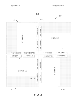
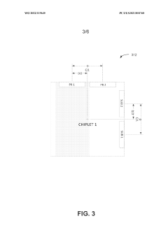
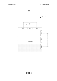
Edge interface placements to enable chiplet rotation into multi-chiplet cluster
PatentWO2022119635A2
Innovation
- The placement of I/O pads at the edges of chiplets in a symmetrical arrangement relative to the centerline, allowing for rotation to achieve proper alignment and close-coupled interconnects, thereby facilitating dense packaging and minimizing the system footprint.
Substrate frame design for three-dimensional stacked electronic assemblies
PatentActiveUS20230420351A1
Innovation
- The substrate frame is divided into multiple frame sections separated by spaces to allow substrates to expand and contract, with the placement of spaces aligned with areas of maximal warpage identified through physical measurements or simulations, including the use of neural networks to optimize the reduction of stress.


Thermal Management Strategies for Chiplet Designs
Thermal management has emerged as a critical challenge in chiplet-based semiconductor designs due to the increased power density and heterogeneous integration of multiple dies. As chiplet architectures continue to evolve, effective thermal solutions become essential for maintaining performance, reliability, and longevity of these advanced semiconductor packages.
The thermal challenges in chiplet designs stem from several factors unique to this architecture. First, the stacking or close placement of multiple dies creates localized hotspots with significantly higher power density than traditional monolithic designs. Second, the interfaces between chiplets introduce thermal resistance that impedes efficient heat dissipation. Third, the heterogeneous nature of chiplets, often combining different process nodes and functionalities, results in non-uniform heat generation patterns.
Current thermal management strategies for chiplet designs can be categorized into passive and active approaches. Passive solutions include advanced thermal interface materials (TIMs) with higher thermal conductivity, optimized heat spreaders, and innovative package-level heat dissipation structures. These materials are continuously evolving, with recent developments in metal-based TIMs showing thermal conductivity improvements of up to 20-30% compared to conventional polymer-based solutions.
Active cooling techniques have also been adapted specifically for chiplet architectures. Microfluidic cooling channels integrated directly into interposers or substrates have demonstrated the ability to handle heat fluxes exceeding 500 W/cm², making them particularly suitable for high-performance computing applications utilizing chiplet designs. Additionally, targeted thermoelectric cooling elements can be strategically placed near known hotspots to provide localized cooling where traditional methods prove insufficient.
Design-time thermal optimization has become increasingly important in the chiplet paradigm. Thermal-aware floorplanning algorithms now consider heat distribution patterns when determining chiplet placement, often resulting in 15-25% lower peak temperatures compared to conventional placement strategies. Similarly, dynamic thermal management techniques have evolved to address the unique characteristics of chiplet designs, with distributed thermal sensors enabling fine-grained power management across different dies.
Industry leaders have developed proprietary thermal solutions for their chiplet products. AMD's Infinity Fabric interconnect architecture incorporates specific thermal design considerations, while Intel's EMIB and Foveros technologies include dedicated thermal management features. These approaches highlight the growing recognition that thermal management must be integrated into the earliest stages of chiplet design rather than addressed as an afterthought.
Looking forward, emerging technologies such as diamond-based heat spreaders, phase-change cooling systems, and AI-driven thermal management algorithms show promise for addressing the escalating thermal challenges as chiplet integration continues to advance toward higher densities and performance levels.
Standardization Efforts in Chiplet Interfaces
The standardization of chiplet interfaces represents a critical development in the semiconductor industry's shift toward disaggregated chip designs. Industry consortia such as the Universal Chiplet Interconnect Express (UCIe) have emerged as pivotal forces in establishing common protocols for chiplet-to-chiplet communication. Founded in 2022 by industry leaders including Intel, AMD, Arm, TSMC, and Samsung, UCIe aims to create an open ecosystem where chiplets from different vendors can seamlessly interoperate.
The UCIe 1.0 specification, released in March 2022, defines both the physical layer and protocol stack for die-to-die interconnection. This standard supports two primary interface modes: a standard package substrate mode operating at 16-32 GT/s and an advanced packaging mode reaching 64-128 GT/s. These specifications enable manufacturers to develop chiplets with standardized interfaces while maintaining flexibility in their internal architectures.
Parallel to UCIe, other significant standardization efforts include JEDEC's Chiplet PHY Express (CPX) and the Open Compute Project's Bunch of Wires (BoW) specification. CPX focuses on memory-centric interconnects, while BoW targets cost-effective integration using existing packaging technologies. The Compute Express Link (CXL) consortium has also extended its focus to include chiplet-level communication protocols, particularly for memory coherency.
The Advanced Interface Bus (AIB) developed by Intel represents another important standard that has gained traction. Now in its third generation, AIB offers an open-source interface specification that several manufacturers have adopted. Similarly, TSMC's Integrated Fan-Out (InFO) and Chip-on-Wafer-on-Substrate (CoWoS) technologies incorporate standardized interface protocols to facilitate multi-vendor chiplet integration.
These standardization efforts face significant technical challenges, including signal integrity at higher bandwidths, power efficiency concerns, and thermal management issues. The industry must balance performance requirements with practical implementation constraints while ensuring backward compatibility with existing systems.
The economic implications of interface standardization are substantial. McKinsey estimates that a mature chiplet ecosystem could reduce design costs by 40-60% and accelerate time-to-market by 30%. However, this requires widespread adoption of common standards rather than fragmentation into competing proprietary interfaces.
Looking forward, the next generation of chiplet interface standards will likely focus on optical interconnects, which promise higher bandwidth and lower power consumption than electrical connections. Research consortia including imec and the Heterogeneous Integration Roadmap team are already developing specifications for silicon photonics integration in chiplet designs, potentially revolutionizing data transfer capabilities between chiplet components.
Unlock deeper insights with PatSnap Eureka Quick Research — get a full tech report to explore trends and direct your research. Try now!
Generate Your Research Report Instantly with AI Agent
Supercharge your innovation with PatSnap Eureka AI Agent Platform!