Designing Gate Drivers For High-Speed GaN HEMTs
SEP 8, 20259 MIN READ
Generate Your Research Report Instantly with AI Agent
Patsnap Eureka helps you evaluate technical feasibility & market potential.
GaN HEMT Gate Driver Technology Evolution and Objectives
Gallium Nitride (GaN) High Electron Mobility Transistors (HEMTs) have emerged as revolutionary power semiconductor devices, offering superior performance compared to traditional silicon-based technologies. The evolution of GaN HEMT technology began in the early 1990s with fundamental research on wide bandgap semiconductors, but it wasn't until the 2000s that commercial applications started to materialize. The inherent properties of GaN, including higher breakdown voltage, faster switching speeds, and lower on-resistance, have positioned these devices as ideal candidates for next-generation power electronics.
The development trajectory of GaN HEMT gate drivers has been closely aligned with the advancement of the transistors themselves. Early gate driver designs were adapted from silicon MOSFET drivers, which proved inadequate for the unique characteristics of GaN HEMTs. The evolution progressed through several key phases: basic adaptation of silicon drivers (2000-2010), specialized GaN-optimized drivers (2010-2015), and the current era of highly integrated, high-performance solutions (2015-present).
A critical turning point in this evolution was the recognition that GaN HEMTs require precise gate voltage control within narrower operating margins compared to silicon devices. Exceeding these margins can lead to device degradation or catastrophic failure. This realization drove the development of gate drivers with tighter voltage regulation, faster transient response, and enhanced protection features.
The technical objectives for modern GaN HEMT gate drivers center around several key parameters. First, minimizing propagation delay and achieving rise/fall times in the sub-nanosecond range to fully leverage GaN's switching speed potential. Second, implementing precise voltage control to maintain gate voltage within the safe operating area, typically +6V/-3V for enhancement-mode devices. Third, incorporating robust protection mechanisms against voltage spikes, oscillations, and shoot-through conditions that are particularly damaging in high-speed switching environments.
Current research trends are focusing on further integration of gate drivers with GaN HEMTs, potentially as monolithic solutions, to minimize parasitic inductances and optimize switching performance. Additionally, there is significant interest in developing intelligent gate drivers with adaptive control algorithms that can dynamically adjust driving parameters based on operating conditions, thereby optimizing efficiency across varying loads and temperatures.
The ultimate goal of GaN HEMT gate driver technology is to enable switching frequencies exceeding 10MHz while maintaining high efficiency and reliability. This would unlock new applications in wireless power transfer, compact RF power amplifiers, and ultra-high-density power converters that were previously unattainable with silicon technology. As the industry continues to push the boundaries of power density and efficiency, the co-evolution of GaN HEMTs and their specialized gate drivers remains a critical enabler for next-generation power electronics.
Market Demand Analysis for High-Speed GaN Power Electronics
The global market for GaN power electronics is experiencing unprecedented growth, driven by the increasing demand for high-efficiency power conversion systems across multiple industries. Current market valuations place the GaN power device sector at approximately 223 million USD in 2023, with projections indicating a compound annual growth rate (CAGR) of 25.8% through 2028, potentially reaching 700 million USD by that time.
This remarkable growth trajectory is primarily fueled by the automotive sector, particularly electric vehicles (EVs), where high-speed switching capabilities and efficiency improvements offered by GaN HEMTs translate directly into extended range and reduced charging times. The automotive power electronics market segment alone is expected to grow at 30% CAGR over the next five years, with GaN-based solutions capturing an increasing share from traditional silicon-based technologies.
Consumer electronics represents another significant market driver, with manufacturers seeking more compact, efficient power adapters and chargers. The transition to USB-C Power Delivery protocols requiring intelligent power management has created substantial demand for advanced gate driver solutions that can maximize GaN HEMT performance while maintaining reliability.
Industrial applications constitute the third major market segment, where high-voltage DC power distribution, motor drives, and renewable energy systems benefit from GaN's superior switching characteristics. The industrial sector's adoption rate is accelerating as system designers become more comfortable with GaN technology and as total cost of ownership advantages become more apparent.
Regional analysis reveals Asia-Pacific as the dominant manufacturing hub, accounting for approximately 65% of GaN power device production, though North America leads in innovation and intellectual property development. Europe shows the fastest growth rate in adoption, driven by stringent efficiency regulations and sustainability initiatives.
Market research indicates that customers prioritize three key factors when selecting GaN power solutions: reliability (cited by 78% of surveyed system designers), performance (68%), and ease of implementation (55%). This highlights the critical importance of gate driver design, as it directly impacts all three factors.
The competitive landscape shows increasing collaboration between semiconductor manufacturers and gate driver specialists, with several strategic partnerships announced in the past 18 months. This trend underscores the recognition that optimized gate driver solutions are essential to unlocking the full potential of GaN technology and capturing market share in this rapidly expanding sector.
Current Challenges in GaN HEMT Gate Driver Design
Despite significant advancements in GaN HEMT technology, gate driver design remains a critical challenge that limits the full exploitation of GaN's superior switching capabilities. The fundamental issue stems from GaN HEMTs' extremely fast switching speeds (dv/dt rates exceeding 100V/ns) and their unique gate characteristics compared to traditional silicon devices. These high switching speeds create substantial common-mode noise that can corrupt gate signals and trigger false turn-on/off events, potentially leading to catastrophic device failures.
One persistent challenge is managing the gate voltage requirements. Unlike silicon MOSFETs with robust gates, GaN HEMTs typically have narrow gate voltage margins (often +6V/-3V) with minimal tolerance for overshoot. Exceeding these limits even momentarily can permanently damage the device, necessitating precise voltage regulation and transient control mechanisms that conventional gate drivers struggle to provide.
The parasitic inductance in gate driver loops presents another significant obstacle. Even minimal inductance (few nH) can create substantial voltage ringing during high-speed switching transitions. This ringing effect is particularly problematic in GaN applications where switching frequencies often exceed 1MHz, creating resonant circuits that amplify noise and compromise signal integrity.
Common-mode transient immunity (CMTI) represents perhaps the most formidable challenge. The isolation barrier in gate drivers must withstand extreme dv/dt rates while maintaining signal integrity. Current optocoupler or transformer-based isolation technologies often exhibit limitations at the CMTI levels required for optimal GaN performance (>100V/ns), creating a technological bottleneck.
Power consumption in gate drivers also presents unique challenges for GaN applications. While GaN HEMTs require less gate charge than comparable silicon devices, the significantly higher switching frequencies increase the dynamic power consumption in gate drivers. This creates thermal management challenges, especially in compact power designs where cooling options are limited.
Layout considerations further complicate GaN gate driver design. The physical arrangement of components becomes critical at high frequencies, with even millimeter-scale differences potentially introducing sufficient parasitic elements to degrade performance. Conventional PCB design approaches often prove inadequate for maintaining signal integrity in these applications.
Finally, there's a growing need for intelligent protection mechanisms specifically tailored to GaN's unique failure modes. Traditional overcurrent protection schemes are often too slow to prevent damage in GaN circuits, which can transition from normal operation to failure in nanoseconds rather than microseconds.
Current Gate Driver Architectures for GaN HEMTs
01 High-speed gate driver circuit designs for GaN HEMTs
Specialized gate driver circuit designs are essential for GaN HEMTs to achieve high-speed switching performance. These circuits incorporate optimized components and layouts to minimize parasitic inductances and capacitances that can limit switching speeds. Advanced topologies include push-pull configurations, bootstrap circuits, and integrated feedback mechanisms that enable precise control of gate voltage transitions, resulting in faster switching speeds and reduced switching losses in high-frequency applications.- High-speed gate driver circuit designs for GaN HEMTs: Specialized gate driver circuit designs are essential for maximizing the switching performance of GaN HEMTs in high-speed applications. These circuits incorporate features like optimized gate resistance, low parasitic inductance paths, and precise timing control to enable fast switching transitions while preventing oscillations. Advanced topologies may include multi-stage driving, adaptive gate voltage control, and integrated protection mechanisms to handle the unique characteristics of GaN devices.
- Integration techniques for GaN HEMT gate drivers: Integration approaches for GaN HEMT gate drivers focus on minimizing parasitic elements and improving thermal management. These techniques include monolithic integration of drivers with power devices, advanced packaging methods, and optimized PCB layouts. By placing the driver closer to the GaN device and using specialized interconnection methods, switching losses are reduced and higher operating frequencies can be achieved, which is critical for high-speed applications.
- Protection and monitoring features for GaN gate drivers: Protection and monitoring systems are crucial for reliable operation of high-speed GaN HEMT gate drivers. These include over-current protection, over-voltage protection, and temperature monitoring circuits that can respond within nanoseconds. Advanced designs incorporate dynamic dead-time adjustment, shoot-through prevention, and fault detection mechanisms specifically tailored to the fast switching characteristics of GaN devices, ensuring safe operation under various conditions.
- Voltage and current control strategies for GaN gate drivers: Specialized voltage and current control strategies are implemented in GaN HEMT gate drivers to optimize switching performance. These include precise control of gate voltage slew rates, active Miller clamp circuits, and dynamic gate current modulation. By carefully managing the gate charge and discharge profiles, these techniques minimize switching losses and electromagnetic interference while enabling operation at very high frequencies required in modern power conversion applications.
- Isolation and level-shifting techniques for GaN gate drivers: Isolation and level-shifting techniques are essential for high-side GaN HEMT gate drivers in bridge configurations. These include high-speed digital isolators, transformer-based isolation, and specialized bootstrap circuits designed for the fast switching speeds of GaN devices. Advanced designs incorporate common-mode transient immunity features and optimized power supply arrangements to maintain signal integrity during high-speed switching events, which is critical for reliable operation in power conversion systems.
02 Gate drive voltage control techniques for GaN HEMTs
Precise control of gate drive voltages is critical for optimizing GaN HEMT performance. These techniques include adaptive voltage control systems that adjust gate drive levels based on operating conditions, multi-level driving schemes that provide different voltage levels during turn-on and turn-off transitions, and voltage clamping mechanisms that protect against gate overvoltage. Such control techniques enable faster switching while maintaining safe operation within the device's voltage limitations.Expand Specific Solutions03 Integration of protection features in GaN HEMT gate drivers
Gate drivers for GaN HEMTs incorporate various protection features to ensure reliable high-speed operation. These include overcurrent protection circuits that rapidly detect and respond to fault conditions, temperature monitoring systems that adjust operation based on thermal feedback, and short-circuit protection mechanisms with fast response times. Advanced designs also feature soft-start capabilities and controlled slew rates to prevent damage during transient conditions while maintaining high switching speeds.Expand Specific Solutions04 Isolation technologies for high-speed GaN HEMT gate drivers
Isolation technologies are crucial for high-speed GaN HEMT gate drivers to prevent noise coupling and ensure signal integrity. These include galvanic isolation using transformers, optocouplers, or capacitive coupling techniques specifically designed for high-frequency operation. Advanced isolation barriers maintain fast signal transmission while providing protection against common-mode transients and voltage spikes, enabling reliable high-speed switching in power conversion applications.Expand Specific Solutions05 Packaging and integration solutions for GaN HEMT gate drivers
Advanced packaging and integration solutions enhance the performance of GaN HEMT gate drivers. These include co-packaged driver and HEMT designs that minimize interconnection parasitics, integrated power modules with optimized thermal management, and 3D packaging technologies that reduce loop inductances. Such integration approaches enable higher switching frequencies, improved thermal performance, and enhanced electromagnetic compatibility, making them ideal for compact high-speed power conversion systems.Expand Specific Solutions
Key Industry Players in GaN Power Semiconductor Ecosystem
The GaN HEMT gate driver design market is in a growth phase, with increasing adoption across power electronics applications. The market is expanding rapidly due to GaN's superior performance over silicon in high-frequency, high-efficiency applications. Technologically, the field shows varying maturity levels, with established semiconductor players like Texas Instruments, ROHM, and Wolfspeed leading commercial development. Taiwan Semiconductor and United Microelectronics provide foundry support, while Qualcomm and Enphase Energy drive application-specific innovations. Research institutions including Indian Institute of Science and University of California contribute to fundamental advancements. The competitive landscape features both specialized GaN-focused companies like Ganpower International and diversified semiconductor manufacturers, with increasing collaboration between academic and industrial sectors to overcome technical challenges in high-speed switching applications.
ROHM Co., Ltd.
Technical Solution: ROHM has developed comprehensive gate driver solutions for GaN HEMTs that address the unique challenges of high-speed switching. Their BM61S40RFV-C gate driver IC is specifically designed for GaN power devices, featuring ultra-fast propagation delays below 25ns to maximize GaN's switching speed advantages. ROHM's approach includes implementing precise dead-time control with nanosecond resolution to prevent shoot-through conditions while minimizing power losses. Their drivers incorporate specialized level-shifting technology that can withstand the high dv/dt rates (>100V/ns) common in GaN applications. ROHM has integrated advanced protection features including undervoltage lockout, overcurrent protection with response times under 200ns, and temperature monitoring. Their gate drivers are designed with optimized internal layout to minimize parasitic inductances, and they provide detailed application guidelines for PCB layout to maintain signal integrity at high switching frequencies. ROHM's solutions also feature adjustable slew rate control to balance EMI performance with switching losses.
Strengths: Extensive experience with wide bandgap semiconductor applications; comprehensive protection features specifically designed for GaN; strong integration capabilities combining drivers with other power management functions. Weaknesses: More limited market presence in some regions compared to larger competitors; some solutions may prioritize robustness over absolute performance metrics; requires careful system design to fully leverage capabilities.
Texas Instruments Incorporated
Technical Solution: Texas Instruments has developed advanced gate driver solutions specifically designed for GaN HEMTs, focusing on optimizing switching performance while addressing the unique challenges of high-speed operation. Their LMG341x family of gate drivers incorporates integrated protection features including overcurrent protection, temperature monitoring, and under-voltage lockout specifically tailored for GaN applications. TI's approach includes careful optimization of the gate drive loop inductance with compact packaging and optimal PCB layout recommendations to minimize parasitic inductances that can cause ringing and EMI issues. Their drivers implement precise control of slew rates with programmable turn-on/turn-off times to balance switching losses and EMI. Additionally, TI has developed specialized level-shifting technology to accommodate the unique voltage requirements of GaN devices, with drivers capable of operating at frequencies exceeding 2MHz while maintaining signal integrity.
Strengths: Comprehensive integration of protection features specifically designed for GaN applications; industry-leading switching frequency capabilities; extensive application support and design resources. Weaknesses: Higher cost compared to basic gate driver solutions; requires careful system design to fully utilize advanced features; some solutions may be overengineered for simpler GaN applications.
Critical Patents and Innovations in GaN Driver Technology
High-side gate driver for gallium nitride integrated circuits
PatentActiveUS10855273B2
Innovation
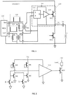
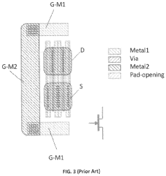
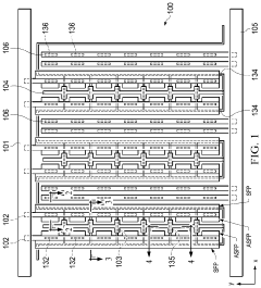
- A gate driver circuit implemented on a GaN monolithic integrated circuit, comprising a RS-flipflop and amplifier, which receives pulse trains and produces a gate driver signal for the GaN power transistor, eliminating the need for separate silicon-based control/drive functional blocks and reducing parasitic inductances by co-packaging the RS-flipflop, amplifier, and GaN power transistor.
Transistor with source field plates and non-overlapping gate runner layers
PatentActiveUS20210143258A1
Innovation
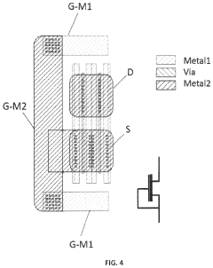
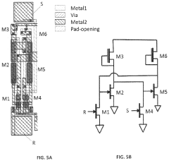
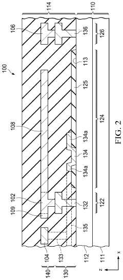
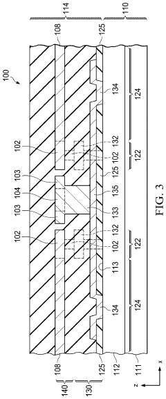
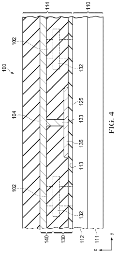
- The design includes a field plate extending from the source runner layer or source contact layer, positioned coplanar with the gate runner layer, allowing it to overlap vertically with the metal gate layer, reducing parasitic capacitance and resistance without additional routings, thus enhancing size efficiency.
Thermal Management Considerations for High-Frequency Operation
Thermal management represents a critical challenge in the design of gate drivers for high-speed GaN HEMTs. As switching frequencies increase beyond the capabilities of traditional silicon devices, the thermal considerations become increasingly complex and demanding. The high-frequency operation of GaN HEMTs can generate significant heat through various loss mechanisms, including switching losses, conduction losses, and gate driver losses.
The thermal behavior of GaN-based power systems differs substantially from silicon counterparts due to the material properties and smaller die sizes. GaN devices typically operate at higher power densities, creating concentrated heat sources that require sophisticated thermal management strategies. Junction temperature control becomes paramount, as GaN HEMTs exhibit performance degradation and reliability concerns when operating above recommended temperature thresholds.
Heat dissipation pathways must be carefully engineered in high-frequency GaN applications. The primary thermal paths include conduction through the device package to the PCB, convection from exposed surfaces, and radiation. Among these, conduction typically dominates, making the thermal interface materials (TIMs) and PCB design critical factors. Advanced TIMs with high thermal conductivity and low thermal resistance are essential for efficient heat transfer from the device to cooling structures.
PCB layout considerations for thermal management include the use of thermal vias, copper pours, and strategic component placement. Multiple thermal vias beneath GaN devices can significantly reduce thermal resistance, while proper copper distribution helps spread heat across larger areas. The gate driver placement relative to the GaN HEMT also impacts thermal performance, as shorter interconnections reduce parasitic inductances but may concentrate heat generation.
Active cooling solutions become necessary for high-power density applications. These range from forced-air cooling with heatsinks to liquid cooling systems for the most demanding scenarios. The selection depends on power levels, ambient conditions, and system constraints. Innovative approaches such as embedded cooling channels and phase-change materials are emerging as potential solutions for next-generation designs.
Thermal simulation and modeling tools play an essential role in predicting hotspots and optimizing thermal designs before physical prototyping. Computational fluid dynamics (CFD) and finite element analysis (FEA) enable designers to evaluate various cooling strategies and identify potential thermal bottlenecks. These tools have become indispensable as operating frequencies push beyond megahertz ranges, where thermal challenges intensify.
Dynamic thermal management techniques, including adaptive gate driving and intelligent power management, represent advanced approaches to balancing performance and thermal constraints. These systems can modulate switching parameters based on temperature feedback, ensuring reliable operation across varying conditions while maximizing performance within thermal limits.
EMI/EMC Challenges and Mitigation Strategies
The integration of Gallium Nitride High Electron Mobility Transistors (GaN HEMTs) into power electronic systems introduces significant electromagnetic interference (EMI) and electromagnetic compatibility (EMC) challenges. These challenges stem primarily from the high switching speeds and steep voltage transitions (dv/dt) that characterize GaN devices, which can reach switching rates exceeding 100 V/ns.
When designing gate drivers for high-speed GaN HEMTs, common-mode noise becomes a critical concern. The rapid voltage transitions create displacement currents through parasitic capacitances, particularly between the power stage and surrounding circuitry. These currents can propagate through the system, causing interference with sensitive control and measurement circuits. Additionally, the high-frequency switching operations generate conducted and radiated emissions that may exceed regulatory standards.
Layout considerations play a crucial role in mitigating EMI/EMC issues. Minimizing loop areas in both power and gate drive circuits reduces parasitic inductance, which otherwise can lead to voltage overshoots and ringing. Implementing proper grounding strategies, such as single-point grounding or ground planes with strategic partitioning between power and signal grounds, helps contain high-frequency noise. Careful placement of components to minimize coupling paths between noise sources and sensitive circuits is equally important.
Shielding techniques represent another essential mitigation strategy. This includes both physical shields for sensitive components and electromagnetic shields for entire circuit sections. In some cases, metal enclosures with appropriate gaskets may be necessary to contain radiated emissions from the GaN-based power stage.
Filter design constitutes a fundamental approach to EMI suppression. Common-mode chokes on input and output lines can significantly reduce conducted emissions. Strategic placement of decoupling capacitors close to the GaN devices helps manage high-frequency noise at its source. Snubber circuits can be employed to dampen voltage overshoots and ringing, though their design must be optimized to avoid compromising the switching performance advantages of GaN technology.
Advanced gate driver designs incorporate features specifically targeting EMI/EMC issues. Controlled slew rates allow designers to balance switching losses against EMI generation. Some gate drivers implement programmable dead-time control to optimize switching transitions while minimizing noise generation. Isolation barriers between the control circuitry and power stage, using technologies such as optical, magnetic, or capacitive isolation, prevent noise propagation through the control path.
Compliance testing methodologies must be adapted for GaN-based systems. Traditional EMC testing procedures may need modification to accurately capture the high-frequency emissions characteristic of GaN switching. Pre-compliance testing during development phases helps identify potential issues early, reducing costly redesigns later in the product development cycle.
Unlock deeper insights with Patsnap Eureka Quick Research — get a full tech report to explore trends and direct your research. Try now!
Generate Your Research Report Instantly with AI Agent
Supercharge your innovation with Patsnap Eureka AI Agent Platform!
