Embedded Sensor Fabrication Via Volumetric Additive Manufacturing
SEP 4, 20259 MIN READ
Generate Your Research Report Instantly with AI Agent
Patsnap Eureka helps you evaluate technical feasibility & market potential.
Embedded Sensor Fabrication Background and Objectives
Embedded sensor fabrication through volumetric additive manufacturing represents a significant advancement in the integration of sensing capabilities directly into structural components. This technology has evolved from traditional manufacturing methods that required separate fabrication and assembly processes for sensors and their host structures. The evolution began with basic embedded electronics in the early 2000s and has progressed to sophisticated in-situ sensor fabrication techniques that we see today.
The development trajectory of embedded sensor fabrication has been shaped by advancements in materials science, particularly in conductive and semi-conductive materials compatible with additive manufacturing processes. Early iterations focused on simple resistive sensors, while recent developments have enabled the creation of complex multi-functional sensors capable of detecting various physical parameters simultaneously.
Volumetric additive manufacturing, as opposed to layer-by-layer approaches, offers unique advantages for sensor embedding by allowing for true three-dimensional fabrication without the constraints of planar deposition. This technique utilizes photopolymerization throughout a volume of resin simultaneously, enabling the creation of intricate internal structures that would be impossible with conventional manufacturing methods.
The primary objective of embedded sensor fabrication via volumetric additive manufacturing is to create seamlessly integrated sensing systems that maintain structural integrity while providing real-time data acquisition capabilities. This integration aims to eliminate the weaknesses associated with traditional sensor attachment methods, such as adhesive degradation, connection failures, and stress concentration points.
Technical goals in this field include developing multi-material printing capabilities that can simultaneously deposit structural and functional materials with precise spatial control. Another critical objective is to achieve high-resolution fabrication of sensing elements with dimensions approaching the microscale, enabling more sensitive and accurate measurements without compromising the host structure's performance.
Research is also focused on expanding the range of detectable parameters beyond the current capabilities, which primarily include strain, temperature, and pressure. Future developments aim to incorporate chemical sensing, biological parameter monitoring, and electromagnetic field detection within additively manufactured components.
The long-term vision for this technology encompasses self-monitoring structures capable of real-time health assessment and predictive maintenance across various industries including aerospace, automotive, medical devices, and infrastructure. This would represent a paradigm shift from periodic inspection regimes to continuous monitoring systems, potentially revolutionizing how we design and maintain critical components and structures.
Market Demand Analysis for Embedded Sensor Technologies
The embedded sensor market is experiencing robust growth driven by the increasing demand for smart and connected devices across multiple industries. The global market for embedded sensors was valued at approximately $11.5 billion in 2022 and is projected to reach $18.7 billion by 2027, representing a compound annual growth rate (CAGR) of 10.2%. This growth trajectory is particularly significant for volumetric additive manufacturing techniques that enable seamless sensor integration.
Industrial automation represents the largest market segment, accounting for nearly 30% of the embedded sensor demand. Manufacturing facilities are increasingly adopting smart sensors to enable predictive maintenance, process optimization, and quality control. The ability to fabricate sensors directly within structural components via volumetric additive manufacturing addresses the critical need for non-intrusive monitoring in complex industrial systems.
The healthcare sector demonstrates the fastest growth rate at 14.3% annually, driven by the rising adoption of wearable medical devices and implantable sensors. Volumetrically manufactured embedded sensors offer unprecedented opportunities for patient monitoring through customized medical devices with integrated sensing capabilities. The market for implantable sensors alone is expected to double in size over the next five years.
Automotive applications constitute another significant market segment, valued at $2.8 billion in 2022. The transition toward autonomous vehicles and advanced driver assistance systems (ADAS) has intensified the demand for embedded sensors that can be integrated directly into vehicle components. Volumetric additive manufacturing enables the production of complex geometries with embedded sensing functionality, addressing the automotive industry's need for space-efficient and reliable sensor solutions.
Consumer electronics represents a high-volume market for embedded sensors, with over 3 billion devices shipped annually containing multiple sensor types. The trend toward miniaturization and increased functionality in smartphones, wearables, and smart home devices creates substantial opportunities for volumetrically manufactured sensors that can be seamlessly integrated into product designs.
Aerospace and defense applications, though smaller in volume, offer high-value opportunities for embedded sensor technologies. The sector's stringent requirements for reliability, durability, and performance in extreme conditions align well with the capabilities of volumetric additive manufacturing processes.
Geographically, North America leads the market with a 35% share, followed by Europe (28%) and Asia-Pacific (25%). However, the Asia-Pacific region is expected to demonstrate the highest growth rate over the next five years due to rapid industrialization and increasing adoption of IoT technologies in countries like China, Japan, and South Korea.
Current State and Challenges in Volumetric Additive Manufacturing
Volumetric Additive Manufacturing (VAM) represents a paradigm shift in 3D printing technology, moving beyond traditional layer-by-layer approaches to enable simultaneous solidification throughout an entire volume. Currently, the global landscape of VAM technology shows significant advancements in research institutions across North America, Europe, and parts of Asia, with the United States and Germany leading in patent filings and academic publications.
The state-of-the-art VAM systems primarily utilize photopolymerization techniques, with computed axial lithography (CAL) and holographic volumetric printing emerging as the dominant approaches. CAL systems project synchronized patterns of light from multiple angles into photosensitive resin, creating complex 3D structures in seconds rather than hours. Recent developments have achieved resolution capabilities approaching 100 microns, with print volumes up to 80 cm³ in laboratory settings.
Despite these advances, VAM faces substantial technical challenges that limit widespread industrial adoption. The foremost challenge remains material compatibility, as current systems predominantly work with specialized photopolymers that often lack the mechanical properties, thermal stability, and biocompatibility required for advanced applications. The integration of functional materials, particularly conductive elements necessary for embedded sensor fabrication, presents significant hurdles due to light scattering and absorption issues.
Resolution limitations constitute another critical challenge. While conventional additive manufacturing can achieve features below 50 microns, volumetric techniques struggle to maintain consistent resolution throughout the build volume, particularly for complex geometries with internal features. This becomes especially problematic for sensor fabrication, where precise dimensional control is paramount.
Scaling production represents a persistent obstacle. Current VAM systems demonstrate impressive speed for small components but encounter difficulties when scaling to larger volumes or higher throughput production. The exponential increase in computational requirements for larger objects creates bottlenecks in real-time projection calculations.
From a manufacturing perspective, process monitoring and quality control mechanisms remain underdeveloped compared to traditional additive manufacturing. The simultaneous solidification throughout the volume complicates in-situ monitoring, making defect detection challenging until post-production inspection.
The integration of multiple materials within a single print process—essential for creating functional embedded sensors—represents perhaps the most significant technical barrier. Current VAM systems typically operate with homogeneous materials, lacking the sophisticated material handling and deposition control needed for multi-material fabrication with distinct electrical, mechanical, and sensing properties.
These challenges are compounded by the nascent state of design tools and simulation software specifically optimized for volumetric manufacturing processes, creating barriers for engineers attempting to leverage this technology for embedded sensor applications.
Current Technical Solutions for Embedded Sensor Fabrication
01 Direct embedding of sensors during volumetric additive manufacturing
Volumetric additive manufacturing techniques allow for direct embedding of sensors within 3D printed structures during the fabrication process. This approach enables the integration of sensing capabilities without interrupting the printing process, resulting in seamless sensor incorporation. The embedded sensors can monitor various parameters such as strain, temperature, or pressure within the structure, providing real-time feedback on the object's condition and performance.- Direct embedding of sensors during volumetric additive manufacturing: Volumetric additive manufacturing techniques allow for the direct embedding of sensors within 3D printed structures during the fabrication process. This approach enables the integration of sensing capabilities without interrupting the printing process, resulting in seamless sensor incorporation. The embedded sensors can monitor various parameters such as strain, temperature, or pressure within the structure, providing real-time feedback on the object's condition or environment.
- Multi-material printing for functional sensor integration: Multi-material volumetric additive manufacturing enables the fabrication of embedded sensors using different materials with varying properties. By strategically depositing conductive, semi-conductive, and insulating materials within a single printing process, functional sensors can be created as integral parts of the printed structure. This approach allows for complex sensor geometries and configurations that would be difficult to achieve using traditional manufacturing methods.
- In-situ curing and polymerization techniques for sensor embedding: Advanced in-situ curing and polymerization techniques enable the creation of embedded sensors during volumetric additive manufacturing. These methods utilize selective photopolymerization, thermal curing, or other solidification processes to create sensing elements within the structure as it is being fabricated. The controlled solidification allows for precise positioning of sensing components within the printed object, enhancing the functionality and reliability of the embedded sensors.
- Voxel-based fabrication for high-resolution sensor integration: Voxel-based volumetric additive manufacturing enables high-resolution integration of sensors within printed structures. By controlling the material properties at the voxel level, sensing elements can be precisely positioned and configured within the object. This approach allows for the creation of complex sensor networks with multiple sensing modalities distributed throughout the printed structure, enhancing the spatial resolution and functionality of the embedded sensing system.
- Post-processing techniques for enhancing embedded sensor performance: Various post-processing techniques can be applied to enhance the performance of sensors embedded during volumetric additive manufacturing. These techniques include thermal annealing, surface treatment, or selective material activation to improve the electrical, mechanical, or sensing properties of the embedded components. Post-processing can also involve the creation of microchannels or cavities within the printed structure to accommodate additional sensing elements or to facilitate the connection of embedded sensors to external electronics.
02 Multi-material printing for functional sensor integration
Multi-material volumetric additive manufacturing enables the fabrication of embedded sensors using different materials with varying properties. By strategically depositing conductive, dielectric, and sensing materials in a single fabrication process, functional sensors can be created within the structure. This approach allows for the creation of complex sensor geometries and networks that would be difficult to achieve using traditional manufacturing methods.Expand Specific Solutions03 In-situ monitoring and calibration of embedded sensors
Advanced volumetric additive manufacturing systems incorporate in-situ monitoring capabilities that allow for real-time calibration and verification of embedded sensors during the fabrication process. This ensures the functionality and accuracy of the sensors before the completion of the manufacturing process. The monitoring systems can detect defects or misalignments in the sensor components and make necessary adjustments to maintain the desired performance characteristics.Expand Specific Solutions04 Hybrid manufacturing approaches for complex sensor systems
Hybrid manufacturing approaches combine volumetric additive manufacturing with other fabrication techniques to create complex embedded sensor systems. These methods may involve pausing the printing process to insert pre-fabricated sensor components, followed by resuming the print to encapsulate the sensors. Alternatively, they may integrate subtractive manufacturing steps to create cavities or channels for sensor placement. Hybrid approaches offer flexibility in sensor design and placement while maintaining the benefits of volumetric additive manufacturing.Expand Specific Solutions05 Post-processing techniques for embedded sensor activation
Various post-processing techniques are employed to activate or enhance the functionality of embedded sensors after the volumetric additive manufacturing process. These techniques include thermal treatment to cure sensing materials, surface modification to improve sensor response, and electrical activation to establish connections between sensor components. Post-processing steps are crucial for ensuring the long-term stability and reliability of embedded sensors in their operating environment.Expand Specific Solutions
Key Industry Players in Volumetric Manufacturing and Sensor Integration
Embedded Sensor Fabrication Via Volumetric Additive Manufacturing is currently in an early growth phase, with the market expanding as industries recognize its potential for creating smart components with integrated sensing capabilities. The global market is estimated to reach $2-3 billion by 2025, driven by applications in aerospace, automotive, and healthcare sectors. Technologically, the field is advancing rapidly but remains in development, with companies at different maturity levels. Industry leaders like EOS GmbH, Renishaw, and Siemens Energy are establishing robust capabilities, while research institutions such as CNRS and Lawrence Livermore National Security are pioneering fundamental innovations. Specialized players like Divergent Technologies and BigRep are developing niche applications, while traditional manufacturing giants including GE, Bosch, and Continental are integrating these technologies into their product ecosystems.
Teknologian Tutkimuskeskus VTT Oy
Technical Solution: VTT Technical Research Centre of Finland has developed innovative approaches to embedded sensor fabrication through volumetric additive manufacturing that focus on hybrid material systems. Their technology combines direct write techniques with traditional AM processes to create multi-material structures with integrated sensing capabilities. VTT's approach utilizes aerosol jet printing to deposit conductive inks and sensing materials at precise locations within a component during the build process. Their process enables the creation of complex 3D electronic circuits and sensing elements embedded within structural materials. A significant innovation is their development of nanocomposite materials that combine structural polymers with functional nanoparticles to create materials that inherently possess sensing capabilities. VTT has demonstrated this technology in applications including smart packaging with embedded humidity sensors, structural health monitoring systems for industrial equipment, and wearable medical devices with integrated biosensors. Their research has shown particular success in creating flexible and stretchable electronics embedded within polymer structures.
Strengths: Excellent compatibility with flexible and stretchable substrates; ability to create highly customized sensing solutions; good scalability for certain applications. Weaknesses: Challenges with long-term reliability in harsh environments; limited compatibility with high-temperature applications; potential issues with signal interference in densely packed sensor networks.
Renishaw Plc
Technical Solution: Renishaw has developed sophisticated embedded sensor fabrication capabilities using their metal powder bed fusion additive manufacturing technology. Their approach focuses on integrating sensing elements within metal components during the build process, creating parts with built-in monitoring capabilities. Renishaw's technology utilizes selective laser melting to create complex metal structures while strategically incorporating cavities and channels for subsequent sensor integration. Their process includes pausing the build at predetermined layers to insert pre-fabricated sensing elements or to deposit specialized functional materials that form the sensing components. A key innovation is their development of hybrid manufacturing cells that combine additive manufacturing with precision machining and automated sensor placement, enabling seamless integration of electronic components within metal structures. This technology has been successfully applied in industrial applications for creating smart tooling with embedded temperature and pressure sensors that provide real-time feedback during manufacturing processes.
Strengths: Excellent for creating robust metal components with integrated sensing; high temperature resistance of embedded sensors; superior mechanical properties of final components. Weaknesses: Limited flexibility in sensor positioning compared to some other methods; challenges in creating truly volumetric sensor networks; higher costs associated with metal AM processes.
Core Patents and Innovations in Volumetric Sensor Integration
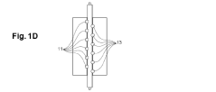
Sensor construction and method for manufacturing an article with an embedded sensor
PatentWO2020201634A1
Innovation
- A sensor construction with a heat insulating material cover protects the sensor from manufacturing temperatures, allowing it to be embedded within metal articles during the process, with access holes for data transmission via RFID antennas or wiring.
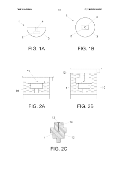
Method for integrating sensor into component fabricated by additive manufacturing
PatentPendingJP2023090695A
Innovation
- A method for integrating sensors into metal components via additive manufacturing that creates a housing volume wider than the sensor, allowing for protection during high-temperature printing processes.
- The formation of melt paddles on both sides of the sensor during the second part of additive printing, which helps secure and protect the sensor within the metal component.
- A two-step additive manufacturing process that enables sensor integration between fabrication stages, allowing for complex sensor-embedded metal components.


Materials Science Advancements for Sensor Embedding Applications
Recent advancements in materials science have significantly expanded the possibilities for embedded sensor fabrication through volumetric additive manufacturing. The development of multi-functional materials with tunable electrical, mechanical, and thermal properties has been crucial in overcoming traditional limitations in sensor embedding processes.
Conductive polymers have emerged as a cornerstone material innovation, offering flexibility and electrical conductivity without compromising structural integrity. These materials, including PEDOT:PSS and polyaniline derivatives, have been reformulated specifically for compatibility with volumetric manufacturing techniques, achieving conductivity values approaching 1000 S/cm while maintaining printability.
Piezoelectric materials have undergone substantial refinement, with new ceramic-polymer composites demonstrating enhanced sensitivity and durability when fabricated through volumetric processes. BaTiO₃-PVDF composites, in particular, have shown excellent response characteristics while being compatible with light-based curing methods essential for volumetric manufacturing.
Metamaterials engineered at the microscale have introduced unprecedented sensing capabilities, including programmable mechanical responses and self-healing properties. These materials incorporate precisely designed microstructures that can be fabricated through computed tomography volumetric printing, enabling sensors with directionally dependent properties.
Smart hydrogels represent another breakthrough, offering stimuli-responsive behavior ideal for biosensing applications. Recent formulations have overcome previous stability limitations, with cross-linking mechanisms specifically designed for volumetric light-based curing that maintain responsiveness to target analytes while providing structural stability.
Nanocomposite materials have dramatically improved the resolution and sensitivity of embedded sensors. Carbon nanotube and graphene-based composites compatible with volumetric manufacturing processes have achieved feature sizes below 10 μm while maintaining excellent electrical properties, enabling highly miniaturized sensing elements.
Interfacial materials science has addressed one of the most persistent challenges in embedded sensor fabrication: ensuring robust connections between dissimilar materials. New gradient-property materials and specialized coupling agents have been developed that can be incorporated directly into the volumetric manufacturing process, eliminating delamination issues that previously plagued multi-material sensors.
These materials science innovations collectively enable a new generation of embedded sensors with improved performance, reliability, and manufacturing scalability, positioning volumetric additive manufacturing as an increasingly viable approach for advanced sensing applications across industries.
Quality Control and Testing Methodologies for Embedded Sensors
Quality control and testing methodologies for embedded sensors manufactured through volumetric additive manufacturing require specialized approaches that differ significantly from traditional sensor testing frameworks. The integration of sensors within complex three-dimensional structures necessitates comprehensive testing protocols that can verify functionality without compromising the integrity of the host material.
Non-destructive testing (NDT) techniques have emerged as critical tools in this domain. Advanced imaging methods such as micro-computed tomography (μCT) and terahertz imaging enable internal inspection of embedded sensors without physical access. These techniques provide valuable data on sensor positioning accuracy, interface quality between sensor and host material, and detection of potential voids or delaminations that could affect performance.
Electrical characterization represents another fundamental testing methodology, encompassing impedance spectroscopy, signal-to-noise ratio assessment, and response time measurements. These tests must be performed both immediately after fabrication and after environmental conditioning to evaluate long-term stability and performance degradation under various operating conditions.
Environmental reliability testing has been developed specifically for embedded sensor systems, subjecting them to thermal cycling, humidity exposure, mechanical loading, and vibration testing. The correlation between environmental stressors and sensor performance degradation provides critical insights into operational limitations and expected service life.
In-situ monitoring during the manufacturing process itself has revolutionized quality control for embedded sensors. Real-time data collection on temperature distribution, curing kinetics, and material flow patterns enables immediate detection of process anomalies that could compromise sensor functionality. This approach has demonstrated significant improvements in first-pass yield rates.
Statistical process control methodologies adapted for volumetric additive manufacturing have been implemented by industry leaders. These frameworks incorporate machine learning algorithms that analyze manufacturing parameters and correlate them with sensor performance metrics, enabling predictive quality control rather than purely reactive testing.
Standardization efforts remain ongoing, with organizations such as ASTM International and IEEE developing specific testing protocols for embedded sensors. These emerging standards address calibration procedures, performance benchmarking, and reliability assessment methodologies tailored to the unique challenges of volumetrically manufactured sensor systems.
Unlock deeper insights with Patsnap Eureka Quick Research — get a full tech report to explore trends and direct your research. Try now!
Generate Your Research Report Instantly with AI Agent
Supercharge your innovation with Patsnap Eureka AI Agent Platform!