Volumetric Additive Manufacturing For Transparent Micro-Optical Elements
SEP 4, 20259 MIN READ
Generate Your Research Report Instantly with AI Agent
Patsnap Eureka helps you evaluate technical feasibility & market potential.
VAM Technology Background and Objectives
Volumetric Additive Manufacturing (VAM) represents a paradigm shift in the field of 3D printing technology, particularly for creating transparent micro-optical elements. Unlike traditional layer-by-layer additive manufacturing approaches, VAM enables the simultaneous solidification of an entire volume of photosensitive resin, offering unprecedented advantages in speed, resolution, and geometric complexity. The evolution of this technology can be traced back to early stereolithography techniques developed in the 1980s, with significant advancements occurring in the past decade through innovations in light projection systems and photochemistry.
The technological trajectory of VAM has been characterized by continuous improvements in spatial resolution, processing speed, and material compatibility. Early iterations were limited by constraints in optical systems and photoinitiator chemistry, resulting in structures with modest resolution. Recent breakthroughs in spatial light modulators, advanced optical designs, and tailored photopolymer formulations have dramatically enhanced capabilities, enabling the fabrication of transparent micro-optical elements with sub-micron features and optical-grade surface quality.
Current research in VAM technology is driven by the growing demand for miniaturized optical components in various high-tech industries, including telecommunications, medical devices, augmented reality, and autonomous vehicles. These applications require optical elements with increasingly complex geometries, high transparency, and precise refractive properties that conventional manufacturing methods struggle to deliver efficiently or economically.
The primary technical objectives for VAM development in the context of transparent micro-optical elements include achieving sub-micron resolution across large build volumes, reducing optical aberrations and scattering in printed structures, developing photopolymer formulations with tunable refractive indices, and ensuring long-term stability of optical properties. Additionally, there is a focus on increasing throughput while maintaining precision, as commercial viability depends on balancing quality with production efficiency.
Future development aims to overcome current limitations in build volume, further enhance resolution, and expand the range of compatible materials with diverse optical properties. Researchers are exploring multi-material VAM systems capable of creating gradient-index optics and hybrid components with integrated functionalities. The ultimate goal is to establish VAM as a mainstream manufacturing technology for next-generation optical systems, enabling designs that were previously impossible or prohibitively expensive to produce.
The convergence of advanced computational methods, including topology optimization and machine learning algorithms, with VAM hardware developments represents a promising frontier for achieving these ambitious technical objectives. This synergistic approach is expected to accelerate innovation in both the process technology and the design possibilities for transparent micro-optical elements.
Market Analysis for Transparent Micro-Optical Elements
The global market for transparent micro-optical elements manufactured through volumetric additive manufacturing is experiencing significant growth, driven by increasing demand across multiple industries. The market size for micro-optical components was valued at approximately $2.3 billion in 2022 and is projected to reach $4.1 billion by 2028, representing a compound annual growth rate of 10.2%.
Consumer electronics represents the largest market segment, accounting for nearly 35% of the total market share. The miniaturization trend in smartphones, wearables, and AR/VR devices has created substantial demand for high-precision transparent optical elements. Apple's investment in micro-optics for their AR glasses and Meta's continued development of VR headsets exemplify this growing market need.
Medical device applications constitute the fastest-growing segment with a 12.8% CAGR. Minimally invasive surgical tools, endoscopes, and diagnostic equipment increasingly rely on miniaturized optical components. The precision offered by volumetric additive manufacturing enables the production of complex optical geometries essential for these applications.
Automotive applications represent another significant market, particularly with the rise of advanced driver-assistance systems (ADAS) and autonomous vehicles. Transparent micro-optical elements are critical components in LiDAR systems, heads-up displays, and sensor arrays. This segment is expected to grow at 11.5% annually through 2028.
Telecommunications and data communications sectors show steady demand growth, particularly for fiber optic components, micro-lenses for laser coupling, and optical switches. The ongoing expansion of 5G infrastructure and increasing data center capacity are key drivers in this segment.
Regional analysis indicates North America currently leads the market with 38% share, followed by Asia-Pacific at 35% and Europe at 22%. However, the Asia-Pacific region is expected to overtake North America by 2026, driven by rapid industrialization in China, South Korea, and Taiwan, and significant investments in advanced manufacturing capabilities.
Customer requirements are evolving toward higher optical performance, greater miniaturization, and increased integration capabilities. The ability to produce complex geometries with high transparency and precise optical properties gives volumetric additive manufacturing a competitive advantage over traditional manufacturing methods.
Market barriers include high initial equipment costs, technical challenges in achieving consistent optical quality, and limited material selection. However, these barriers are gradually being overcome through continued technological advancements and increasing adoption across industries.
Current VAM Challenges for Optical Transparency
Despite significant advancements in Volumetric Additive Manufacturing (VAM) technologies, achieving optical transparency in micro-optical elements remains a formidable challenge. The primary obstacle lies in the material properties and processing techniques that often introduce optical imperfections. Conventional photopolymers used in VAM typically exhibit inherent light scattering due to heterogeneous polymerization, resulting in refractive index variations throughout the printed structure.
Material selection presents a significant hurdle, as most commercially available resins for VAM are optimized for mechanical properties rather than optical clarity. The photopolymerization process itself introduces molecular-level inhomogeneities that manifest as optical aberrations in the final product. These microscopic variations, though negligible for structural applications, become critical limitations when producing optical elements requiring precise light transmission characteristics.
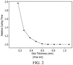
Resolution limitations further compound the transparency challenge. Current VAM systems typically achieve feature resolutions in the range of 10-50 micrometers, which approaches but does not fully satisfy the requirements for high-quality micro-optical elements where sub-micron precision is often necessary. This resolution constraint leads to surface roughness that causes light scattering and reduces transparency.
Post-processing techniques to enhance transparency remain underdeveloped for VAM-produced components. Unlike traditional manufacturing methods where polishing can improve optical quality, the complex geometries enabled by VAM often preclude conventional finishing approaches. Chemical treatments that might enhance transparency frequently compromise the dimensional accuracy or structural integrity of the printed elements.
The multi-material capabilities essential for advanced optical systems with gradient refractive indices or specialized optical properties are still in their infancy within VAM technologies. Current systems struggle to seamlessly integrate multiple transparent materials with precisely controlled interfaces, limiting the functional complexity of printable optical elements.
Scalability presents another significant challenge. While laboratory demonstrations have shown promising results for small-scale transparent optical elements, scaling these processes for commercial production while maintaining optical quality remains problematic. The balance between production speed and optical quality creates a technological bottleneck that has yet to be resolved.
Characterization and quality control methodologies specific to transparent VAM products are also underdeveloped. The industry lacks standardized testing protocols to evaluate optical performance metrics such as transmittance, scattering, and wavefront distortion in complex 3D-printed optical geometries, making it difficult to benchmark improvements and ensure consistent quality.
Material selection presents a significant hurdle, as most commercially available resins for VAM are optimized for mechanical properties rather than optical clarity. The photopolymerization process itself introduces molecular-level inhomogeneities that manifest as optical aberrations in the final product. These microscopic variations, though negligible for structural applications, become critical limitations when producing optical elements requiring precise light transmission characteristics.
Resolution limitations further compound the transparency challenge. Current VAM systems typically achieve feature resolutions in the range of 10-50 micrometers, which approaches but does not fully satisfy the requirements for high-quality micro-optical elements where sub-micron precision is often necessary. This resolution constraint leads to surface roughness that causes light scattering and reduces transparency.
Post-processing techniques to enhance transparency remain underdeveloped for VAM-produced components. Unlike traditional manufacturing methods where polishing can improve optical quality, the complex geometries enabled by VAM often preclude conventional finishing approaches. Chemical treatments that might enhance transparency frequently compromise the dimensional accuracy or structural integrity of the printed elements.
The multi-material capabilities essential for advanced optical systems with gradient refractive indices or specialized optical properties are still in their infancy within VAM technologies. Current systems struggle to seamlessly integrate multiple transparent materials with precisely controlled interfaces, limiting the functional complexity of printable optical elements.
Scalability presents another significant challenge. While laboratory demonstrations have shown promising results for small-scale transparent optical elements, scaling these processes for commercial production while maintaining optical quality remains problematic. The balance between production speed and optical quality creates a technological bottleneck that has yet to be resolved.
Characterization and quality control methodologies specific to transparent VAM products are also underdeveloped. The industry lacks standardized testing protocols to evaluate optical performance metrics such as transmittance, scattering, and wavefront distortion in complex 3D-printed optical geometries, making it difficult to benchmark improvements and ensure consistent quality.
Current VAM Solutions for Transparent Elements
01 Transparent materials for volumetric additive manufacturing
Various transparent materials can be used in volumetric additive manufacturing to create objects with optical clarity. These materials include specific photopolymers, resins, and composites that maintain transparency after curing. The formulations often contain photoinitiators that respond to specific wavelengths while preserving optical clarity in the final printed part. These materials enable the production of transparent components for optical applications, medical devices, and visualization models.- Transparent materials for volumetric additive manufacturing: Various transparent materials can be used in volumetric additive manufacturing to create objects with optical clarity. These materials include specific photopolymers, resins, and composites that maintain transparency after curing. The formulations often contain photoinitiators that respond to specific wavelengths while preserving optical clarity throughout the printing process. These materials enable the production of transparent parts with complex internal structures that would be difficult to achieve with traditional manufacturing methods.
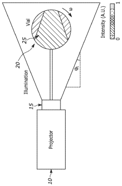
- Light projection techniques for transparent volumetric printing: Advanced light projection systems are essential for volumetric additive manufacturing of transparent objects. These systems use precisely controlled light patterns, often from multiple angles or with tomographic approaches, to selectively cure photosensitive resins while maintaining transparency. Techniques include computed axial lithography, holographic projection, and synchronized multi-beam systems that minimize light scattering and maintain optical clarity throughout the build volume. These methods allow for the creation of transparent structures without the layer lines typical in conventional 3D printing.
- Post-processing methods for enhancing transparency: Various post-processing techniques can significantly improve the transparency of volumetrically printed objects. These methods include surface polishing, thermal treatments, chemical baths, and specialized coatings that reduce surface roughness and internal light scattering. Some processes involve infiltration with index-matching materials or controlled reflow of the polymer surface. These post-processing steps are crucial for achieving optical-grade transparency in volumetrically manufactured components for applications requiring high optical clarity.
- Transparent functional components for optical applications: Volumetric additive manufacturing enables the creation of transparent functional components for various optical applications. These include custom lenses, waveguides, light pipes, optical sensors, and microfluidic devices with integrated optical elements. The technology allows for embedding functional elements within transparent structures and creating gradient-index optics with spatially varying properties. These capabilities open new possibilities for integrated optics, biomedical imaging devices, and custom optical instruments that would be difficult to produce using conventional manufacturing methods.
- Process control for consistent transparency: Maintaining consistent transparency in volumetric additive manufacturing requires sophisticated process control systems. These systems monitor and adjust parameters such as light intensity, exposure time, resin temperature, and curing dynamics in real-time. Advanced algorithms compensate for light scattering and absorption effects that could compromise transparency. Some systems incorporate in-situ monitoring with optical feedback to ensure uniform curing throughout the volume. These control mechanisms are essential for producing transparent parts with reproducible optical properties and minimal internal defects.
02 Light projection techniques for transparent volumetric printing
Advanced light projection methods are essential for creating transparent objects in volumetric additive manufacturing. These techniques include computed tomography-inspired approaches, holographic projections, and synchronized multi-angle illumination systems. By carefully controlling light delivery throughout the entire volume of photosensitive resin, these methods can produce complex transparent structures with minimal optical distortion and high geometric accuracy, eliminating the need for layer-by-layer processing.Expand Specific Solutions03 Post-processing methods for enhancing transparency
Various post-processing techniques can significantly improve the transparency of volumetrically printed objects. These methods include specialized curing processes, surface treatments, polishing techniques, and thermal processing. By removing surface irregularities and ensuring complete polymerization throughout the printed object, these post-processing steps can enhance optical clarity, reduce light scattering, and improve overall transparency of the manufactured components.Expand Specific Solutions04 Tomographic approaches for transparent volumetric printing
Tomographic volumetric additive manufacturing techniques enable the creation of transparent objects by projecting computed patterns of light into photosensitive resin. These approaches use algorithms to calculate the necessary light patterns from multiple angles, creating fully formed objects in seconds rather than hours. The tomographic methods allow for the production of complex transparent structures with high resolution and minimal internal stress, resulting in superior optical properties compared to traditional layer-by-layer printing methods.Expand Specific Solutions05 Resin formulations with tunable optical properties
Specialized resin formulations have been developed with tunable optical properties specifically for volumetric additive manufacturing. These formulations contain carefully selected monomers, oligomers, and additives that can be adjusted to control refractive index, light transmission, and other optical characteristics. By manipulating the chemical composition and curing conditions, manufacturers can create transparent printed objects with customized optical properties for specific applications such as lenses, light guides, and optical sensors.Expand Specific Solutions
Leading Companies in Micro-Optical Manufacturing
Volumetric Additive Manufacturing for transparent micro-optical elements is currently in an early growth phase, with increasing market interest driven by applications in medical devices, consumer electronics, and automotive sectors. The market size is projected to expand significantly as the technology matures from laboratory demonstrations to commercial applications. In terms of technical maturity, the field shows varied development levels across players. EssilorLuxottica and FUJIFILM are leveraging their optical expertise to advance commercial applications, while research institutions like EPFL and Lawrence Livermore National Laboratory are pioneering fundamental breakthroughs. Specialized additive manufacturing companies such as Carbon, Formlabs, and Readily3D are developing proprietary volumetric printing technologies specifically for transparent optical elements, with Readily3D's tomographic approach showing particular promise for high-resolution, rapid fabrication of optical components.
École Polytechnique Fédérale de Lausanne
Technical Solution: EPFL has pioneered a volumetric additive manufacturing technique called "Computed Axial Lithography" (CAL) specifically optimized for transparent micro-optical elements. Their approach projects synchronized patterns of light into a rotating volume of photosensitive resin, creating complex 3D structures without the need for supports or layers. EPFL researchers have achieved printing speeds of less than 30 seconds for complete optical components with feature sizes down to 80 micrometers while maintaining over 95% light transmission in the visible spectrum. Their technology incorporates computational optimization algorithms that predict and compensate for light scattering and absorption effects during the printing process, resulting in highly precise optical surfaces. EPFL has also developed specialized photopolymer formulations with tunable refractive indices (ranging from 1.4 to 1.7) specifically designed for optical applications, enabling the creation of gradient-index optics and complex lens arrays in a single manufacturing step.
Strengths: Exceptional optical clarity with minimal post-processing requirements; ability to create complex freeform optics impossible with traditional manufacturing; rapid production capabilities suitable for both prototyping and small-batch production. Weaknesses: Current build volumes remain relatively small (under 5cm³); requires sophisticated computational resources for pattern generation; technology still primarily in research phase rather than full commercial deployment.
Lawrence Livermore National Security LLC
Technical Solution: Lawrence Livermore National Laboratory (LLNL) has developed an advanced volumetric additive manufacturing technology called "Computed Axial Lithography" (CAL) specifically optimized for transparent micro-optical elements. Their approach projects computed tomographic images into a rotating volume of photosensitive resin, allowing the entire 3D structure to be created simultaneously rather than layer-by-layer. LLNL's implementation achieves printing speeds of less than 60 seconds for complete optical components with feature resolution down to 50 micrometers while maintaining over 98% optical transparency. Their technology incorporates sophisticated algorithms that account for light scattering, refraction, and absorption effects during the printing process, resulting in highly precise optical surfaces with minimal post-processing requirements. LLNL has also developed specialized photopolymer formulations with controlled refractive indices and low shrinkage properties specifically designed for optical applications, enabling the creation of complex optical elements such as microlens arrays, waveguides, and diffractive optical elements in a single manufacturing step.
Strengths: Exceptional optical clarity due to absence of layer lines; ability to create complex internal geometries impossible with traditional manufacturing; extremely fast production times compared to conventional methods; access to advanced materials science capabilities. Weaknesses: Technology primarily focused on research applications rather than commercial production; requires sophisticated computational resources for pattern generation; currently limited build volumes compared to some industrial systems.
Key Patents in Transparent Optical Printing
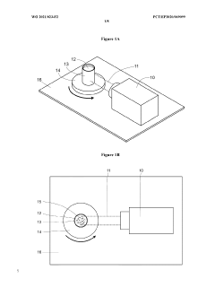
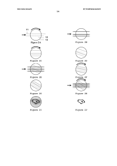
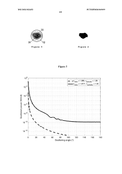
Method of volumetric additive manufacturing
PatentWO2024069272A1
Innovation
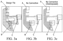
- The method involves rotating a vial of photocurable resin and projecting structured light images to cure only the shell and interior scaffolding of the object, using infilling and deconvolution to correct for diffusion effects, ensuring uniform curing of all features without over-exposure.
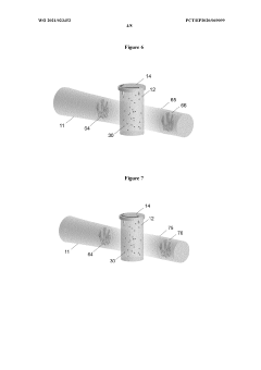
Method and apparatus for volumetric additive manufacturing of cell-loaded resins
PatentWO2021023452A1
Innovation
- The method involves adjusting the refractive index of the photoresponsive material to match that of the scattering particles and using a light source emitting wavelengths longer than 630 nm, such as between 630 nm to 1050 nm, to reduce light scattering and achieve optimal print accuracy and resolution.
Material Science Advancements for Optical Applications
Recent advancements in material science have significantly propelled the development of transparent micro-optical elements through volumetric additive manufacturing. Traditional optical materials like glass and polymers have been reimagined with novel compositions and structures that enhance their optical properties while maintaining compatibility with advanced manufacturing techniques. Particularly noteworthy is the emergence of hybrid organic-inorganic materials that combine the processability of polymers with the optical stability of inorganic compounds.
Photopolymerizable resins have undergone substantial refinement, with new formulations achieving refractive indices exceeding 1.7 while maintaining over 95% transparency in the visible spectrum. These materials incorporate specialized monomers and photoinitiators that enable precise control over the curing process during volumetric manufacturing, resulting in homogeneous optical properties throughout the printed structure. The addition of nanoparticles such as titanium dioxide and zirconium oxide has proven effective in modulating refractive indices without compromising transparency.
Silica-based materials have also seen remarkable progress, with sol-gel processes adapted for volumetric printing applications. These materials offer exceptional thermal stability and resistance to environmental degradation, critical factors for optical elements in demanding applications. Recent research has demonstrated the successful incorporation of rare-earth dopants into these matrices, enabling the creation of active optical elements with luminescent or amplification properties directly during the manufacturing process.
The development of multi-material systems represents another frontier in optical materials science. Gradient-index optics, previously difficult to manufacture, can now be produced through controlled spatial variation of material composition during volumetric printing. This capability enables the creation of optical elements with continuously varying refractive indices, eliminating interfaces that cause reflection losses and aberrations in conventional optics.
Self-healing materials are emerging as a promising direction for enhancing the durability of printed optical elements. These materials incorporate dynamic chemical bonds that can reform after damage, maintaining optical clarity over extended periods. Initial demonstrations have shown recovery of up to 85% of original optical transmission after surface scratching, significantly extending the functional lifetime of micro-optical components in practical applications.
Biocompatible optical materials represent another significant advancement, particularly relevant for biomedical applications. These materials combine optical transparency with physiological compatibility, enabling the direct printing of optical sensors or imaging elements for in vivo applications. Recent formulations have achieved both FDA-approved biocompatibility and the optical precision required for micro-scale imaging applications.
Quality Control Methods for Micro-Optical Elements
Quality control in volumetric additive manufacturing (VAM) for transparent micro-optical elements presents unique challenges due to the microscale dimensions and optical performance requirements. Traditional inspection methods often prove inadequate for these specialized components, necessitating advanced metrology solutions tailored to micro-optical applications.
Surface quality assessment represents a critical aspect of quality control for transparent micro-optical elements. Techniques such as white light interferometry and atomic force microscopy enable nanometer-level surface roughness measurements, which directly impact optical performance. For VAM-produced components, maintaining surface roughness below 10nm is typically required to minimize light scattering effects that would otherwise compromise optical clarity.
Dimensional accuracy verification employs confocal microscopy and optical coherence tomography to evaluate the geometric fidelity of printed micro-optical elements. These non-contact methods can detect deviations as small as 0.1μm, ensuring that critical optical parameters such as radius of curvature and aspheric coefficients meet design specifications. Automated measurement systems increasingly incorporate machine learning algorithms to accelerate inspection processes while maintaining measurement precision.
Optical performance testing constitutes the definitive quality assessment for transparent micro-optical elements. Modulation transfer function (MTF) analysis quantifies image quality by measuring contrast transfer across spatial frequencies. Wavefront sensing techniques detect optical aberrations by comparing actual light propagation against theoretical models. These measurements provide direct validation of functional performance rather than merely inferring it from geometric parameters.
Material homogeneity evaluation addresses the unique challenges of volumetric printing processes. Polarimetry and photoelastic stress analysis can detect internal stress patterns that may cause birefringence effects. Refractive index mapping across the printed volume ensures uniform optical properties, as variations exceeding 0.0001 can significantly impact performance in precision applications such as microscopy objectives or endoscopic lenses.
In-process monitoring systems represent the frontier of quality control for VAM. Real-time optical coherence tomography during printing allows for immediate detection of defects, while spectroscopic techniques monitor photopolymerization kinetics to ensure complete curing. These approaches enable closed-loop control systems that can adjust process parameters dynamically, significantly reducing rejection rates and improving manufacturing consistency for high-value micro-optical components.
Unlock deeper insights with Patsnap Eureka Quick Research — get a full tech report to explore trends and direct your research. Try now!
Generate Your Research Report Instantly with AI Agent
Supercharge your innovation with Patsnap Eureka AI Agent Platform!