Volumetric Additive Manufacturing In Lab-On-A-Chip Devices
SEP 4, 20259 MIN READ
Generate Your Research Report Instantly with AI Agent
Patsnap Eureka helps you evaluate technical feasibility & market potential.
VAM Technology Background and Objectives
Volumetric Additive Manufacturing (VAM) represents a paradigm shift in fabrication technology, evolving from traditional layer-by-layer 3D printing approaches to simultaneous solidification of entire volumes. This revolutionary technique has emerged over the past decade as researchers sought to overcome speed limitations and resolution constraints inherent in conventional additive manufacturing methods. VAM utilizes principles of computed tomography in reverse, projecting patterned light into photosensitive resins to create complex three-dimensional structures in seconds rather than hours.
The integration of VAM with Lab-on-a-Chip (LOC) devices marks a significant technological convergence. LOC systems, which miniaturize laboratory functions onto small platforms, have traditionally faced manufacturing challenges due to their intricate microfluidic channels, valves, and sensing components. Conventional fabrication methods often require complex multi-step processes, limiting design flexibility and increasing production costs.
The historical trajectory of this technology begins with early demonstrations of volumetric printing using intersecting laser beams in the early 2000s, followed by significant breakthroughs around 2017-2019 when researchers at Lawrence Livermore National Laboratory and UC Berkeley demonstrated high-resolution volumetric fabrication using computed axial lithography. Concurrently, microfluidic technology has evolved from simple channel designs to sophisticated integrated systems requiring increasingly complex fabrication approaches.
The primary objective of VAM in LOC applications is to enable rapid, single-step fabrication of complex three-dimensional microfluidic architectures with features spanning from nanometers to centimeters. This technology aims to overcome the planar limitations of traditional lithography-based approaches while maintaining precision at the microscale. Specific goals include achieving sub-micron resolution in critical features, reducing fabrication time from days to minutes, and enabling previously impossible geometries such as fully enclosed channels with variable cross-sections.
Additional technical objectives include developing biocompatible and optically transparent resin formulations specifically designed for LOC applications, creating software tools that translate microfluidic design requirements into optimized light projection patterns, and establishing standardized processes that ensure reproducibility across different manufacturing setups. The ultimate aim is to democratize complex microfluidic device fabrication, making custom LOC devices accessible to researchers without specialized cleanroom facilities.
The convergence of these technologies promises to revolutionize fields ranging from point-of-care diagnostics to organ-on-chip platforms for drug development, representing a significant opportunity for innovation at the intersection of additive manufacturing and microfluidic engineering.
Market Analysis for Lab-on-a-Chip Applications
The global lab-on-a-chip (LOC) market is experiencing robust growth, valued at approximately $8.2 billion in 2023 and projected to reach $16.5 billion by 2028, representing a compound annual growth rate (CAGR) of 15.1%. This significant expansion is driven by increasing demand for point-of-care diagnostics, personalized medicine, and miniaturized analytical systems across healthcare, pharmaceutical, and environmental monitoring sectors.
The integration of volumetric additive manufacturing (VAM) into LOC devices represents a particularly promising market segment. Healthcare applications dominate the current market landscape, accounting for nearly 45% of the total LOC market share, with diagnostic applications being the primary driver. The pharmaceutical industry follows closely, utilizing LOC platforms for drug discovery and development processes, representing approximately 30% of market applications.
Regional analysis reveals North America as the current market leader with 38% market share, followed by Europe (28%) and Asia-Pacific (25%). However, the Asia-Pacific region is demonstrating the fastest growth rate at 17.3% CAGR, driven by increasing healthcare infrastructure investments in China and India, along with strong government support for biotech innovation.
Key market drivers include the growing prevalence of chronic diseases necessitating rapid diagnostic solutions, increasing demand for point-of-care testing, and the push toward personalized medicine approaches. The COVID-19 pandemic has further accelerated market growth by highlighting the critical importance of rapid, accessible diagnostic technologies.
Consumer demand patterns indicate strong preference for LOC devices offering multiple functionalities, reduced sample volume requirements, faster analysis times, and seamless integration with existing laboratory workflows. The incorporation of VAM technology specifically addresses these demands by enabling complex 3D microstructures within chips, enhancing functionality while maintaining cost-effectiveness.
Market challenges include regulatory hurdles, with approval processes varying significantly across regions, creating barriers to global market entry. Additionally, high initial development costs for VAM-integrated LOC devices and technical challenges in ensuring reproducibility at scale represent significant market constraints.
Emerging opportunities include the development of LOC devices for environmental monitoring applications, projected to grow at 18.2% CAGR, and increasing adoption in veterinary medicine. The integration of artificial intelligence and machine learning capabilities with LOC platforms represents another high-growth potential segment, particularly for data analysis and interpretation from complex VAM-enabled microfluidic structures.
Current VAM Challenges in Microfluidics
Despite the promising potential of Volumetric Additive Manufacturing (VAM) in microfluidic applications, several significant technical challenges currently impede its widespread implementation in Lab-on-a-Chip (LOC) devices. The primary obstacle remains resolution limitations, as most commercial VAM systems achieve feature sizes of 50-100 μm, whereas many microfluidic applications require sub-10 μm precision for effective functionality. This resolution gap represents a fundamental barrier to creating truly functional microfluidic components with complex internal geometries.
Material compatibility presents another substantial challenge, as biocompatible photopolymers suitable for both VAM processing and biological applications remain limited. Current materials often exhibit cytotoxicity or poor optical transparency, compromising their utility in diagnostic and analytical applications. Additionally, many VAM-compatible materials lack the mechanical properties necessary for withstanding pressure in microfluidic operations or demonstrate poor long-term stability when exposed to biological samples.
Process integration difficulties further complicate VAM implementation in microfluidics. The seamless incorporation of VAM-fabricated components with traditional microfluidic manufacturing processes, such as soft lithography or injection molding, remains problematic. Interface issues between different materials and manufacturing methods often result in leakage points or structural weaknesses that compromise device performance.
Surface quality control represents a persistent challenge, as VAM-produced microchannels frequently exhibit surface roughness that can disrupt fluid flow, cause unwanted particle adhesion, or create nucleation sites for bubbles. This roughness stems from the layer-by-layer nature of the manufacturing process and the optical scattering effects inherent in volumetric projection systems.
Throughput limitations also constrain industrial adoption, with current VAM technologies requiring significant processing time for high-resolution microfluidic structures. This time-intensive nature makes VAM less competitive compared to traditional mass production methods for microfluidic chips, particularly for commercial applications requiring high-volume manufacturing.
Post-processing requirements further complicate the workflow, as VAM-produced microfluidic devices often need additional treatment steps to remove uncured resin from internal channels or to achieve desired surface properties. These steps add complexity and time to the manufacturing process, reducing the overall efficiency advantage of VAM.
Finally, characterization and quality control of internal microfluidic features remain challenging, as conventional inspection methods struggle to assess the integrity of enclosed microchannels and chambers. This verification gap creates uncertainty in device performance and reliability, particularly for complex microfluidic architectures with intricate internal geometries that are otherwise impossible to fabricate using traditional methods.
Current VAM Integration Solutions for LOC Devices
01 Light-based volumetric additive manufacturing techniques
Light-based volumetric additive manufacturing involves using photopolymerization to create 3D objects in a single step. This technique uses projected light patterns or holographic methods to cure entire volumes of photosensitive resin simultaneously, rather than layer by layer. The process significantly reduces production time compared to traditional additive manufacturing methods and enables the creation of complex geometries without support structures. Advanced optical systems and specialized photopolymers are key components of these systems.- Volumetric additive manufacturing techniques: Volumetric additive manufacturing involves creating three-dimensional objects by solidifying material throughout a volume simultaneously, rather than layer by layer. These techniques include computed axial lithography, tomographic volumetric additive manufacturing, and holographic approaches that use light patterns to cure photosensitive resins. This approach enables faster production times compared to traditional layer-by-layer methods and can create complex geometries without support structures.
- Materials for volumetric additive manufacturing: Various materials are used in volumetric additive manufacturing, including photosensitive resins, hydrogels, and composite materials. These materials are formulated with specific photoinitiators and absorbers to control light penetration and curing characteristics. Advanced formulations enable the creation of objects with gradient properties, functional components, and biocompatible structures suitable for medical applications. The development of these materials focuses on improving mechanical properties, resolution, and processing speed.
- Light projection systems for volumetric manufacturing: Light projection systems are crucial components in volumetric additive manufacturing, using digital light processing (DLP), spatial light modulators, or holographic techniques to project patterned light into photosensitive materials. These systems can generate complex 3D light distributions through computed tomography principles, enabling the simultaneous solidification of material throughout a volume. Advanced optical setups incorporate multiple light sources, beam steering mechanisms, and synchronization systems to achieve high resolution and uniform curing throughout the build volume.
- Process control and optimization in volumetric manufacturing: Process control and optimization in volumetric additive manufacturing involve sophisticated algorithms for light dose calculation, exposure timing, and material property prediction. These systems use feedback mechanisms to monitor and adjust manufacturing parameters in real-time, ensuring consistent part quality. Computational models simulate light propagation through the resin volume, accounting for scattering, absorption, and refractive effects. Machine learning approaches optimize process parameters based on desired part characteristics, material properties, and production requirements.
- Applications and integration of volumetric manufacturing: Volumetric additive manufacturing is being applied across various industries including medical, aerospace, and consumer products. In the medical field, it enables the rapid production of patient-specific implants, tissue engineering scaffolds, and anatomical models. Industrial applications include the creation of complex components with internal features that would be difficult to produce using traditional manufacturing methods. These systems are being integrated with other manufacturing processes and digital workflows to enable end-to-end production solutions, from design to finished product.
02 Materials and formulations for volumetric printing
Specialized materials and formulations are essential for successful volumetric additive manufacturing. These include photopolymer resins with specific curing characteristics, nanocomposites that enhance mechanical properties, and multi-functional monomers that enable precise control over the curing process. Some formulations incorporate oxygen inhibition control mechanisms to improve resolution and surface quality. Advanced materials can also provide functional properties such as conductivity, biocompatibility, or thermal resistance to the final printed objects.Expand Specific Solutions03 Tomographic volumetric manufacturing systems
Tomographic volumetric manufacturing systems use computed tomography principles to create 3D objects. These systems project multiple 2D patterns from different angles into a photosensitive resin, creating interference patterns that selectively cure specific volumes. The approach allows for high-resolution printing with minimal mechanical movement and can produce complex internal structures that would be difficult to achieve with conventional methods. Advanced algorithms optimize the projection patterns to achieve desired material properties and structural integrity.Expand Specific Solutions04 Hybrid volumetric manufacturing approaches
Hybrid volumetric manufacturing combines multiple additive manufacturing techniques to leverage their respective advantages. These approaches may integrate volumetric printing with traditional layer-by-layer methods, or combine different energy sources such as light and heat. Some systems incorporate post-processing steps directly into the manufacturing workflow. Hybrid approaches can overcome limitations of individual techniques, enabling improved resolution, material versatility, or production speed while maintaining the benefits of volumetric fabrication.Expand Specific Solutions05 Control systems and computational methods for volumetric manufacturing
Advanced control systems and computational methods are crucial for volumetric additive manufacturing. These include sophisticated algorithms for generating optimal projection patterns, real-time feedback systems that monitor and adjust the manufacturing process, and simulation tools that predict material behavior during curing. Machine learning approaches can optimize process parameters based on desired part characteristics. Computational methods also address challenges such as light scattering, refractive effects, and thermal management to improve print quality and consistency.Expand Specific Solutions
Leading Companies in VAM and Microfluidic Technologies
Volumetric Additive Manufacturing (VAM) in Lab-On-A-Chip devices represents an emerging technology at the intersection of 3D printing and microfluidics, currently in its early growth phase. The market is expanding rapidly with projections suggesting significant growth as healthcare and biotech industries adopt these technologies. While the technology is advancing, it remains in the developmental stage with varying degrees of maturity across applications. Leading players include Lawrence Livermore National Security and École Polytechnique Fédérale de Lausanne pioneering fundamental research, Readily3D commercializing tomographic bioprinting solutions, established manufacturers like Formlabs and Stratasys adapting their technologies for microscale applications, and research institutions such as University of California and SINTEF driving innovation through collaborative projects. The convergence of semiconductor expertise from companies like SK Hynix and GLOBALFOUNDRIES with biomedical capabilities is accelerating technological development in this specialized field.
Lawrence Livermore National Security LLC
Technical Solution: Lawrence Livermore National Security (LLNS) has pioneered advanced volumetric additive manufacturing techniques for lab-on-a-chip applications through their Computed Axial Lithography (CAL) technology. This approach uses synchronized rotation of photosensitive resin while projecting computed light patterns to create complex 3D microstructures in seconds rather than hours. LLNS has specifically adapted this technology for biomedical microfluidics by developing specialized formulations that maintain biocompatibility while achieving feature resolutions below 50 microns. Their system incorporates real-time optical feedback mechanisms that adjust projection patterns during fabrication to compensate for optical distortions, ensuring high precision in critical microfluidic components. The technology enables the creation of complex internal geometries impossible with traditional layer-by-layer approaches, including embedded sensors, gradient structures, and functional valves within a single manufacturing step.
Strengths: Exceptional speed (100x faster than conventional methods for certain structures); ability to create truly volumetric parts without support structures; excellent for creating embedded channels and complex internal geometries. Weaknesses: Currently limited to photopolymer materials; requires specialized optical systems that increase initial equipment costs; still working to achieve sub-10 micron resolution needed for some advanced microfluidic applications.
École Polytechnique Fédérale de Lausanne
Technical Solution: École Polytechnique Fédérale de Lausanne (EPFL) has developed an innovative volumetric additive manufacturing technology specifically for lab-on-a-chip applications through their Laboratory of Applied Photonics Devices. Their approach utilizes tomographic volumetric printing that creates entire 3D structures simultaneously rather than layer-by-layer. The technology employs synchronized rotation of a container filled with photosensitive resin while projecting computed light patterns from multiple angles, allowing complete structures to form in seconds rather than hours. EPFL has pioneered specialized biocompatible resins with tunable mechanical properties that maintain optical clarity after curing, critical for lab-on-a-chip applications requiring optical detection methods. Their system achieves feature resolutions down to 15 microns and can create complex internal geometries impossible with traditional manufacturing methods, including embedded channels, valves, and functional components directly within microfluidic devices without assembly steps.
Strengths: Extremely rapid fabrication times (under 30 seconds for complete structures); excellent optical properties in printed parts; ability to create complex internal geometries without support structures. Weaknesses: Currently limited to photopolymer materials; requires specialized optical systems increasing initial equipment costs; technology still scaling to achieve sub-10 micron resolution needed for some advanced applications.
Key Patents in Volumetric Printing for Microfluidics
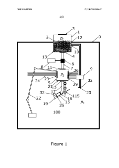
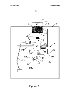
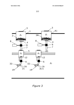
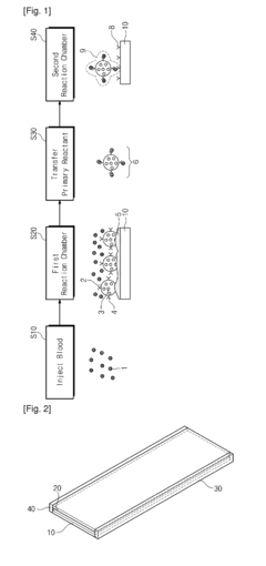
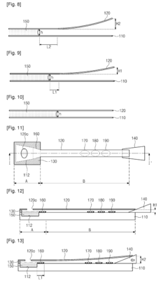
An auxiliary device and a method for volumetric additive manufacturing
PatentWO2020127856A1
Innovation
- A device with an inlet, measurement, and application chamber, equipped with a pneumatic powder transfer system and electrification capabilities, allowing powder material to be transferred and electrically charged or polarized for manipulation within the volumetric printing volume from any direction, using multiaxial mechanizations for precise positioning.
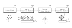
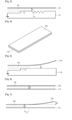
Lab-on-a-chip and method of driving the same
PatentInactiveUS8394595B2
Innovation
- A capillary force lab-on-a-chip design with a gap adjusting mechanism, utilizing a flexible substrate and electromagnets to control the capillary force by adjusting the gap between substrates, allowing for precise control of fluid flow and reaction time through the use of a wedge-shaped gap adjusting member driven by a step motor or electromagnets.
Materials Science Considerations for Biocompatible VAM
The selection of materials for Volumetric Additive Manufacturing (VAM) in lab-on-a-chip applications requires careful consideration of biocompatibility factors to ensure both functionality and safety. Biocompatible materials must maintain their integrity while interfacing with biological samples without causing adverse reactions or contamination. Primary considerations include cytotoxicity, immunogenicity, and long-term stability in biological environments.
Polymeric materials represent the most widely used substrate category for biocompatible VAM applications. Photocurable hydrogels such as polyethylene glycol diacrylate (PEGDA) and gelatin methacrylate (GelMA) have emerged as leading candidates due to their tunable mechanical properties and excellent biocompatibility profiles. These materials can be formulated with varying crosslinking densities to achieve specific mechanical characteristics while maintaining cell viability.
Surface chemistry plays a crucial role in determining how biomolecules and cells interact with VAM-fabricated microfluidic structures. Hydrophilicity, surface charge, and functional group presentation significantly impact protein adsorption and cellular adhesion. Recent advances in surface modification techniques allow for post-fabrication treatments that can enhance biocompatibility without compromising structural integrity.
Photoinitiator selection represents another critical consideration, as these compounds must efficiently initiate polymerization while exhibiting minimal cytotoxicity. Lithium phenyl-2,4,6-trimethylbenzoylphosphinate (LAP) and Irgacure 2959 have demonstrated acceptable biocompatibility profiles at concentrations required for effective VAM processing, though research continues to develop alternatives with improved safety margins.
The mechanical properties of VAM materials must be carefully balanced to meet both manufacturing and application requirements. Materials must possess sufficient rigidity to maintain microfluidic channel geometries while offering appropriate elasticity for applications involving fluid manipulation or cellular interactions. This balance becomes particularly challenging when designing multi-material systems where interfaces between different materials can create potential failure points.
Degradation kinetics represent another important consideration, particularly for applications involving long-term cell culture or implantable devices. Materials must maintain structural integrity for the intended duration of use while potentially offering controlled degradation in specific applications. The degradation products must themselves be non-toxic and easily cleared from the biological system.
Recent research has focused on developing composite materials that combine the processability advantages of synthetic polymers with the bioactivity of natural materials. These hybrid systems aim to provide enhanced cell attachment, proliferation, and differentiation capabilities while maintaining the precision manufacturing advantages of VAM techniques.
Scaling and Commercialization Pathways
The commercialization of Volumetric Additive Manufacturing (VAM) in Lab-on-a-Chip (LOC) devices requires strategic planning to transition from laboratory research to market-ready products. Current scaling approaches focus on parallel processing systems that can simultaneously fabricate multiple microfluidic components, significantly increasing production throughput while maintaining precision.
Investment pathways for commercialization typically follow a staged approach, beginning with research grants and academic-industrial partnerships, followed by venture capital funding as the technology demonstrates commercial viability. Strategic collaborations between microfluidic specialists, materials scientists, and medical device manufacturers have proven essential for successful market entry.
Market adoption barriers include regulatory challenges, particularly for medical applications where FDA or equivalent approvals are required. The integration of VAM into existing manufacturing workflows presents another hurdle, necessitating compatibility with established quality control systems and production lines. Cost considerations remain significant, as initial capital investment for high-resolution VAM equipment can be substantial.
Several business models are emerging in this space. The equipment provider model focuses on selling VAM systems to research institutions and manufacturing facilities. Alternatively, the service bureau approach offers on-demand fabrication services for custom LOC devices. Licensing models, where core VAM technologies are licensed to established manufacturers, provide another pathway with reduced capital requirements.
Time-to-market considerations vary by application sector. Diagnostic applications typically face longer commercialization timelines due to regulatory requirements, while research tools can reach markets more rapidly. Industrial applications often require extensive validation periods to ensure reliability and reproducibility at scale.
Regional innovation clusters are forming around this technology, with notable hubs in Boston, San Francisco, Singapore, and Zurich. These clusters benefit from proximity to academic research centers, manufacturing expertise, and investment capital. Government initiatives supporting advanced manufacturing technologies have accelerated commercialization in these regions through targeted funding programs and regulatory support.
Standardization efforts are underway to establish common protocols for VAM in microfluidic applications, which will be crucial for widespread adoption. Industry consortia are developing specifications for materials compatibility, dimensional tolerances, and quality assurance methodologies specific to VAM-produced LOC devices.
Unlock deeper insights with Patsnap Eureka Quick Research — get a full tech report to explore trends and direct your research. Try now!
Generate Your Research Report Instantly with AI Agent
Supercharge your innovation with Patsnap Eureka AI Agent Platform!