

VAM Approaches For Microfluidic Device Fabrication
SEP 3, 20259 MIN READ
Generate Your Research Report Instantly with AI Agent
PatSnap Eureka helps you evaluate technical feasibility & market potential.
VAM Technology Background and Objectives
Vacuum-Assisted Micromolding (VAM) technology has emerged as a significant advancement in the field of microfluidic device fabrication over the past two decades. This approach represents a convergence of traditional microfabrication techniques with vacuum-assisted processes, enabling more precise control over microstructure formation and material integration. The evolution of VAM technology can be traced back to early experiments with soft lithography in the late 1990s, which laid the groundwork for more sophisticated molding techniques in microfluidics.
The fundamental principle of VAM involves the application of negative pressure during the molding process to eliminate air bubbles, ensure complete filling of microcavities, and achieve high-fidelity replication of microstructures. This technique has progressively evolved from simple vacuum-assisted PDMS (Polydimethylsiloxane) molding to more complex multi-material and multi-layer fabrication approaches that incorporate various polymers, hydrogels, and even biological materials.
Recent technological trends in VAM show a clear movement toward higher precision, automation, and integration with complementary fabrication methods. The development of hybrid approaches combining VAM with 3D printing, laser ablation, or injection molding represents the cutting edge of this technology. Additionally, there is growing interest in scalable VAM processes that can bridge the gap between laboratory prototyping and industrial production of microfluidic devices.
The primary objectives of VAM technology development are multifaceted. First, there is a push toward enhancing resolution capabilities to fabricate structures at sub-micron scales while maintaining high aspect ratios. Second, researchers aim to expand material compatibility to include a wider range of polymers, composites, and biomaterials with specific functional properties. Third, there is significant interest in developing VAM processes that enable the seamless integration of different functional components such as electrodes, sensors, and actuators within microfluidic platforms.
Another critical objective is the standardization of VAM processes to ensure reproducibility and reliability across different fabrication settings. This includes the development of standardized protocols, quality control measures, and characterization methods specific to VAM-fabricated devices. Furthermore, there is a growing emphasis on making VAM technology more accessible and user-friendly, reducing the expertise barrier that currently limits its widespread adoption in various research and industrial settings.
Looking forward, the technological trajectory of VAM approaches is expected to focus on sustainability, with increased attention to environmentally friendly materials and energy-efficient processes. The integration of computational modeling and machine learning algorithms to optimize VAM parameters represents another promising direction for advancing this technology toward more precise and automated microfluidic device fabrication.
Market Analysis for Microfluidic Device Applications
The global microfluidics market has experienced significant growth, valued at approximately $20.7 billion in 2022 and projected to reach $58.8 billion by 2030, with a compound annual growth rate (CAGR) of 13.9%. This robust expansion is driven by increasing applications across multiple sectors, particularly in healthcare, pharmaceuticals, and life sciences.
Healthcare applications dominate the microfluidic device market, accounting for over 45% of the total market share. Point-of-care diagnostics represents the fastest-growing segment within healthcare, with devices enabling rapid, on-site testing for various conditions including infectious diseases, cardiac markers, and blood chemistry analysis. The COVID-19 pandemic has further accelerated adoption of microfluidic-based diagnostic platforms due to their portability and quick results.
Pharmaceutical and biotechnology sectors constitute the second-largest application area, where microfluidic devices are extensively used for drug discovery, high-throughput screening, and personalized medicine development. The ability of microfluidic systems to precisely control small volumes of fluids has revolutionized drug testing procedures, reducing costs by up to 70% compared to traditional methods while increasing throughput by 40-60%.
Environmental monitoring applications are emerging as a promising growth sector, with microfluidic devices being deployed for water quality testing, air pollution monitoring, and soil analysis. This segment is expected to grow at a CAGR of 15.2% through 2030, driven by increasing environmental regulations and sustainability initiatives worldwide.
Industrial applications, including chemical synthesis, material processing, and quality control, represent approximately 12% of the current market. The adoption of microfluidic technologies in these sectors is primarily driven by efficiency gains, with companies reporting 30-50% reductions in reagent consumption and processing time.
Regionally, North America leads the market with approximately 38% share, followed by Europe (29%) and Asia-Pacific (24%). However, the Asia-Pacific region is projected to witness the highest growth rate, driven by increasing healthcare expenditure, expanding research infrastructure, and government initiatives supporting advanced manufacturing technologies in countries like China, Japan, and South Korea.
Consumer demand trends indicate a growing preference for portable, user-friendly devices that offer rapid results with minimal technical expertise required. This has led to the development of smartphone-integrated microfluidic platforms and simplified user interfaces, expanding the potential user base beyond traditional laboratory settings to include clinics, field operations, and even home use.
Current VAM Challenges in Microfluidics
Despite significant advancements in Vat Additive Manufacturing (VAM) for microfluidic device fabrication, several critical challenges persist that limit its widespread industrial adoption. The primary technical obstacle remains resolution limitations, particularly when fabricating microchannels with dimensions below 100 μm. Current VAM systems struggle to consistently produce the fine features required for advanced microfluidic applications, especially when complex geometries with high aspect ratios are needed.
Material compatibility presents another significant hurdle. Many commercially available photopolymer resins used in VAM processes exhibit biocompatibility issues, making them unsuitable for medical and biological applications. Additionally, these materials often demonstrate poor optical transparency, chemical resistance, and mechanical stability under flow conditions, which are essential properties for functional microfluidic devices.
Process repeatability and standardization remain elusive in VAM microfluidic fabrication. The sensitivity of photopolymerization to environmental factors such as ambient temperature, humidity, and light exposure creates significant batch-to-batch variations. This inconsistency hampers quality control and makes scaling to mass production particularly challenging, especially when precise channel dimensions are critical for device performance.
Post-processing requirements constitute a substantial bottleneck in the manufacturing workflow. Uncured resin removal from narrow microchannels presents particular difficulty, often requiring specialized techniques and equipment. Furthermore, surface roughness resulting from the layer-by-layer fabrication process can significantly impact fluid flow characteristics, necessitating additional post-processing steps that increase production time and cost.
Integration challenges with other materials and components further complicate VAM approaches. Creating hybrid devices that combine printed microfluidic structures with sensors, electrodes, or other functional elements remains technically demanding. The interface between printed and non-printed components frequently becomes a failure point due to material incompatibility or bonding issues.
Economic barriers also impede wider adoption, with high-resolution VAM systems requiring substantial capital investment. The specialized nature of biocompatible resins drives material costs significantly higher than conventional manufacturing materials. These economic factors, combined with the technical limitations, create a challenging landscape for implementing VAM in commercial microfluidic device production.
Addressing these challenges requires interdisciplinary research efforts spanning materials science, process engineering, and microfluidic design. Recent developments in hybrid manufacturing approaches and new photopolymer formulations show promise, but significant work remains to overcome these fundamental limitations.
Current VAM Fabrication Methodologies
01 Vertical additive manufacturing systems and equipment
Vertical additive manufacturing (VAM) systems are designed with specialized equipment that enables the building of structures in a vertical orientation. These systems typically include vertical motion platforms, material deposition mechanisms, and control systems that coordinate the building process. The vertical orientation allows for the creation of taller structures with reduced footprint requirements compared to traditional horizontal additive manufacturing approaches.- Vertical additive manufacturing systems and methods: Vertical additive manufacturing (VAM) systems involve building objects in a vertical direction, layer by layer. These systems typically include specialized printing heads, material delivery mechanisms, and control systems that enable precise deposition of materials along the vertical axis. VAM approaches allow for the creation of tall structures with minimal support requirements and can be particularly advantageous for architectural and large-scale industrial applications.
- Material considerations in vertical additive manufacturing: The selection and formulation of materials play a crucial role in vertical additive manufacturing. Materials must possess specific rheological properties to maintain structural integrity during the vertical building process. This includes quick-setting capabilities, appropriate viscosity, and strength characteristics that prevent sagging or deformation while layers are being added. Advanced composite materials, polymers, and specialized concrete formulations are commonly used in VAM applications.
- Control systems and monitoring for VAM processes: Sophisticated control systems are essential for successful vertical additive manufacturing. These systems incorporate real-time monitoring, feedback mechanisms, and adaptive algorithms to ensure precise material deposition and maintain dimensional accuracy throughout the build process. Advanced sensors monitor parameters such as material flow rate, curing conditions, and structural stability, allowing for adjustments during printing to optimize quality and prevent failures.
- Support strategies and structural considerations in VAM: Vertical additive manufacturing requires specialized approaches to structural support and stability. Various techniques have been developed to address the challenges of building vertically without excessive support structures, including gradient material properties, strategic reinforcement placement, and innovative design approaches that leverage the natural strength of certain geometries. These strategies help minimize material usage while ensuring the structural integrity of the printed object.
- Applications and industry-specific VAM implementations: Vertical additive manufacturing has been adapted for various industry-specific applications, including construction, aerospace, and large-scale manufacturing. These implementations often feature customized equipment, specialized material formulations, and process parameters tailored to specific use cases. VAM approaches have been successfully employed in creating architectural elements, infrastructure components, and industrial structures that would be challenging to produce using conventional manufacturing methods.
02 Materials and formulations for VAM processes
Specific materials and formulations are developed for vertical additive manufacturing to address the unique challenges of building in a vertical orientation. These materials must have appropriate viscosity, curing properties, and structural integrity to support their own weight during the building process. Advanced polymer composites, quick-setting concrete mixtures, and specialized metal alloys are among the materials engineered specifically for VAM applications.Expand Specific Solutions03 Control systems and software for vertical building
Sophisticated control systems and software algorithms are essential for successful vertical additive manufacturing. These systems manage the precise deposition of materials, monitor structural integrity during building, and adjust parameters in real-time to ensure dimensional accuracy. Advanced path planning algorithms account for gravity effects and material behavior specific to vertical orientation, while monitoring systems track critical parameters throughout the building process.Expand Specific Solutions04 Structural support strategies for vertical printing
Vertical additive manufacturing requires innovative approaches to structural support during the building process. Various techniques have been developed to address the challenges of gravity and material stability in vertical orientation. These include temporary support structures, gradient material properties, strategic curing methods, and hybrid manufacturing approaches that combine additive and subtractive processes to maintain structural integrity throughout the build.Expand Specific Solutions05 Applications and industry-specific VAM implementations
Vertical additive manufacturing has been adapted for various industry-specific applications. In construction, VAM enables the on-site printing of walls and structural elements. In aerospace, it allows for the creation of complex, lightweight components with internal features. Medical applications include patient-specific implants and prosthetics. Other implementations include infrastructure repair, architectural features, and specialized industrial components that benefit from the unique capabilities of vertical building orientation.Expand Specific Solutions
Leading Companies in Microfluidic VAM Fabrication
The microfluidic device fabrication market is currently in a growth phase, with increasing adoption across biomedical, pharmaceutical, and analytical applications. The market size is projected to expand significantly due to rising demand for point-of-care diagnostics and lab-on-chip technologies. Regarding technical maturity, various approaches exist along the development spectrum. Academic institutions like MIT, Caltech, and University of Maryland are pioneering fundamental research, while established companies such as Corning, STMicroelectronics, and Samsung Electronics are commercializing mature technologies. Specialized players like Hummingbird Nano and PharmaFluidics are bridging innovation gaps with novel fabrication methods. Research organizations including IMEC and Max Planck Society are advancing next-generation techniques, creating a competitive landscape balanced between academic innovation and industrial implementation.
California Institute of Technology
Technical Solution: Caltech has developed a groundbreaking VAM approach for microfluidic device fabrication through their innovative "Microsolidics" platform. This technology combines advanced 3D printing techniques with specialized photopolymerizable materials to create complex microfluidic architectures with unprecedented precision. Their process utilizes a proprietary multi-material projection microstereolithography system that enables the fabrication of fully integrated microfluidic devices with feature sizes down to 5 μm. Caltech's approach incorporates gradient material properties that can be programmed across the device, allowing for localized control of surface chemistry, mechanical properties, and optical characteristics. Their technology enables the creation of truly three-dimensional microfluidic networks with embedded functional components such as valves, pumps, and mixers in a single fabrication step. Caltech researchers have demonstrated applications in single-cell analysis platforms, organ-on-chip systems, and point-of-care diagnostic devices that leverage the unique capabilities of their VAM approach to achieve functionality not possible with conventional fabrication methods.
Strengths: Exceptional resolution and precision; ability to create true 3D microfluidic networks; seamless integration of multiple functional components in a single fabrication process. Weaknesses: Currently limited to smaller device footprints; higher material costs compared to traditional methods; requires specialized equipment not widely available in standard laboratories.
Interuniversitair Micro-Electronica Centrum VZW
Technical Solution: IMEC has developed sophisticated VAM approaches for microfluidic device fabrication centered around their advanced nanoimprint lithography (NIL) and laser-assisted techniques. Their proprietary process combines high-precision molding with specialized polymer materials engineered specifically for microfluidic applications. IMEC's technology enables the creation of multi-layered microfluidic structures with feature sizes down to 50 nanometers, significantly surpassing conventional fabrication methods. Their approach incorporates vertical integration of different functional materials, allowing for the embedding of sensors, electrodes, and optical components directly within the microfluidic channels. IMEC has pioneered a roll-to-roll compatible process that enables high-throughput manufacturing while maintaining nanoscale precision, making their VAM approach particularly suitable for commercial applications. Their technology has been demonstrated in various applications including next-generation sequencing platforms, high-throughput cell sorting devices, and integrated lab-on-chip diagnostic systems with multiplexed detection capabilities.
Strengths: Industry-leading resolution capabilities; established manufacturing processes suitable for commercial scaling; strong integration with electronic components enabling smart microfluidic systems. Weaknesses: Higher initial equipment investment costs; requires specialized expertise for implementation; some proprietary materials have limited shelf life and special handling requirements.
Key Patents and Innovations in VAM Microfluidics
Systems and methods for improved volumetric additive manufacturing
PatentPendingUS20240217180A1
Innovation
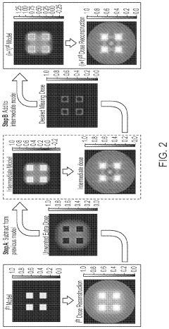
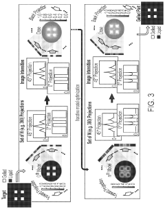
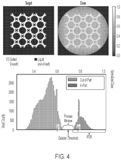
- An algebraic object-space optimization algorithm that directly optimizes image computation for VAM, allowing for improved reconstruction fidelity, simplicity, and flexibility, and enabling new printing geometries and materials like Grayscale VAM, which controls polymeric conversion throughout a printed part.
Manufacture of a microfluidic component by additive manufacturing
PatentWO2019097490A1
Innovation
- The use of additive manufacturing, specifically three-dimensional printing, to create microfluidic components with ceramic bodies and microfluidic structures, allowing for precise definition and reliability of fluid pathways, and the incorporation of thermally conductive ceramics for inertness and mechanical robustness.
Materials Science Considerations for VAM
Materials science plays a critical role in the development and implementation of Vat Additive Manufacturing (VAM) approaches for microfluidic device fabrication. The selection of appropriate photopolymer resins fundamentally determines the physical, chemical, and biological properties of the resulting microfluidic devices.
Photopolymer formulations for VAM typically consist of monomers, oligomers, photoinitiators, and various additives that influence the curing process and final material properties. The viscosity of these resins must be carefully controlled to ensure proper flow during the printing process while maintaining sufficient resolution for microfluidic features. Typically, viscosities between 0.1-10 Pa·s at operating temperatures provide optimal balance between flow characteristics and feature definition.
Mechanical properties of cured VAM materials significantly impact microfluidic device functionality. Young's modulus values ranging from 0.5-3 GPa are common for standard VAM resins, though specialized formulations can achieve either higher rigidity or greater flexibility depending on application requirements. Surface hardness, measured by Shore D hardness typically between 65-85, affects wear resistance and durability during repeated use cycles.
Optical transparency represents another crucial consideration, particularly for applications requiring visual or spectroscopic monitoring of fluid flow. Transmittance values exceeding 85% in the visible spectrum (400-700 nm) are generally desired for analytical applications. Refractive indices typically range from 1.45-1.55, which must be considered when designing optical detection systems integrated with microfluidic platforms.
Chemical compatibility with biological samples and reagents presents significant challenges for VAM-fabricated microfluidic devices. Leaching of uncured monomers or photoinitiator fragments can interfere with biological assays or cell cultures. Surface modification techniques such as plasma treatment, silanization, or polymer grafting are often employed to enhance biocompatibility or introduce specific surface functionalities.
Thermal properties, including glass transition temperature (Tg) and coefficient of thermal expansion (CTE), influence device performance across operating temperature ranges. Most VAM resins exhibit Tg values between 45-120°C, with CTEs typically in the range of 50-100 ppm/°C, which must be considered when designing devices for temperature-sensitive applications.
Recent advances in materials science have led to the development of specialized VAM resins incorporating nanoparticles, conductive elements, or stimuli-responsive components, enabling advanced functionalities such as integrated sensing, actuation, or selective permeability within microfluidic architectures.
Scalability and Cost Analysis of VAM Technologies
The economic viability of VAM (Vat Additive Manufacturing) technologies for microfluidic device fabrication depends significantly on their scalability and cost structure. Current analysis indicates that while initial investment costs for VAM equipment remain relatively high—ranging from $3,000 for entry-level systems to over $100,000 for industrial-grade machines—the per-unit production costs decrease substantially as production volume increases, making it increasingly competitive with traditional fabrication methods.
Material costs represent a critical factor in the economic equation of VAM technologies. Photopolymer resins used in VAM processes typically cost between $150-500 per liter, which is considerably higher than materials used in conventional methods. However, the precision of VAM processes results in minimal material waste, with utilization rates often exceeding 90% compared to 40-60% for traditional subtractive manufacturing techniques.
Energy consumption analysis reveals that VAM technologies demonstrate favorable efficiency metrics, consuming approximately 30-50% less energy per unit compared to injection molding when producing small to medium batch sizes. This advantage diminishes as production volumes increase beyond 10,000 units, where traditional methods benefit from economies of scale.
The labor requirements for VAM processes show significant advantages, with setup and operation requiring 40-60% less skilled labor hours compared to traditional microfluidic fabrication techniques. This reduction stems from the highly automated nature of VAM processes and the elimination of multiple manufacturing steps that characterize conventional approaches.
Infrastructure requirements present another dimension of cost consideration. VAM technologies can be deployed in standard laboratory environments with minimal specialized infrastructure, requiring approximately 50-70% less dedicated space compared to traditional manufacturing setups. This flexibility enables decentralized production models that can further reduce logistics costs.
Time-to-market analysis demonstrates that VAM approaches can reduce development cycles by 60-80% compared to traditional methods, allowing for rapid iteration and customization. This agility translates into significant indirect cost savings through accelerated product development and faster response to market demands.
For scaling considerations, current VAM technologies show optimal economic performance for production volumes ranging from prototypes to approximately 5,000 units. Beyond this threshold, hybrid manufacturing approaches that combine VAM for complex components with traditional methods for simpler elements often yield the most cost-effective solution for large-scale microfluidic device production.
Unlock deeper insights with PatSnap Eureka Quick Research — get a full tech report to explore trends and direct your research. Try now!
Generate Your Research Report Instantly with AI Agent
Supercharge your innovation with PatSnap Eureka AI Agent Platform!