Exploration of Microfluidic Chips in High-Resolution Imaging Applications
OCT 10, 202510 MIN READ
Generate Your Research Report Instantly with AI Agent
Patsnap Eureka helps you evaluate technical feasibility & market potential.
Microfluidic Imaging Background and Objectives
Microfluidic technology has evolved significantly over the past three decades, transforming from simple channel designs to sophisticated integrated systems capable of manipulating fluids at the microscale level. The convergence of microfluidics with high-resolution imaging represents a particularly promising frontier, enabling unprecedented visualization and analysis of biological processes at cellular and subcellular levels.
The historical trajectory of microfluidic imaging began in the early 1990s with rudimentary flow chambers, progressing through polydimethylsiloxane (PDMS) soft lithography techniques in the early 2000s, to today's advanced multi-layer chip designs incorporating various functional elements. This technological evolution has been driven by demands from life sciences, diagnostics, and pharmaceutical research for more precise, dynamic, and high-throughput imaging capabilities.
Current microfluidic imaging systems face several limitations, including optical aberrations at fluid-solid interfaces, limited depth of field, and challenges in maintaining stable sample positioning during high-resolution imaging. These constraints have spurred innovation in chip design, materials science, and integration with advanced microscopy techniques.
The primary objective of exploring microfluidic chips in high-resolution imaging applications is to develop next-generation platforms that overcome existing limitations while expanding functional capabilities. Specifically, we aim to enhance spatial resolution beyond the current 100-200 nm barrier, improve temporal resolution for capturing rapid biological events, and enable multi-modal imaging within the same microfluidic environment.
Recent technological trends indicate movement toward three key directions: integration of adaptive optics to correct for aberrations in real-time; development of transparent, biocompatible materials with optimal refractive indices; and incorporation of AI-driven image processing algorithms to extract maximum information from acquired data.
The potential impact of advanced microfluidic imaging extends across multiple fields. In cancer research, these technologies could enable real-time visualization of tumor cell migration and drug responses. For neuroscience, they offer possibilities for high-resolution imaging of neural networks in controlled microenvironments. In pharmaceutical development, they promise more efficient drug screening through improved visualization of cellular responses.
As we look toward future developments, the convergence of microfluidics with emerging technologies such as optogenetics, super-resolution microscopy, and machine learning algorithms presents exciting opportunities for transformative advances in biological imaging and analysis, potentially revolutionizing our understanding of cellular processes and disease mechanisms.
Market Analysis for High-Resolution Microfluidic Applications
The global market for microfluidic chips in high-resolution imaging applications is experiencing robust growth, driven by increasing demand across multiple sectors including healthcare, pharmaceuticals, and life sciences research. Current market valuations indicate that the microfluidic devices market reached approximately 20 billion USD in 2022, with the segment dedicated to imaging applications representing about 15% of this total. Industry analysts project a compound annual growth rate (CAGR) of 11-13% for the period 2023-2028.
Healthcare applications dominate the market landscape, accounting for nearly 40% of the total demand. Within this sector, point-of-care diagnostics and personalized medicine initiatives are creating substantial opportunities for microfluidic imaging technologies. The pharmaceutical industry follows closely, representing approximately 30% of market share, where high-resolution microfluidic imaging facilitates drug discovery processes and reduces development timelines.
Regional analysis reveals North America as the current market leader with approximately 38% market share, followed by Europe (27%) and Asia-Pacific (25%). However, the Asia-Pacific region is expected to witness the fastest growth rate over the next five years, primarily due to increasing healthcare infrastructure investments in China, Japan, and India, coupled with the expansion of biotechnology research facilities.
Customer segmentation shows research institutions and academic laboratories as early adopters, while clinical diagnostics centers and pharmaceutical companies represent the fastest-growing customer segments. End-user preferences increasingly favor integrated systems that combine microfluidic handling with advanced imaging capabilities, creating a shift toward comprehensive solution providers rather than component manufacturers.
Key market drivers include the growing need for rapid and accurate diagnostic tools, increasing research activities in cell biology, and the shift toward miniaturized analytical systems. The COVID-19 pandemic has further accelerated market growth by highlighting the importance of rapid diagnostic technologies and point-of-care testing solutions.
Market challenges primarily revolve around high initial investment costs, technical complexity in system integration, and regulatory hurdles for clinical applications. The average development cost for a market-ready microfluidic imaging system ranges between 2-5 million USD, creating significant barriers to entry for smaller companies.
Emerging market opportunities include the development of portable high-resolution imaging systems for field applications, integration with artificial intelligence for automated image analysis, and expansion into environmental monitoring and food safety testing markets. These adjacent markets are projected to add an additional 3-4 billion USD to the total addressable market by 2027.
Current Challenges in Microfluidic Chip Imaging Technology
Despite significant advancements in microfluidic chip technology for high-resolution imaging applications, several critical challenges persist that impede optimal performance and widespread adoption. The integration of microfluidic platforms with sophisticated imaging systems faces fundamental physical constraints related to optical accessibility. The materials commonly used in chip fabrication, such as polydimethylsiloxane (PDMS) and polymethyl methacrylate (PMMA), often exhibit autofluorescence and light scattering properties that can significantly compromise image quality and resolution, particularly in fluorescence-based imaging techniques.
Dimensional constraints present another significant hurdle. The miniaturized nature of microfluidic channels, typically ranging from 10-500 micrometers, creates difficulties in achieving adequate focal depth and field of view simultaneously. This becomes particularly problematic when attempting to image dynamic processes occurring at different depths within the microfluidic environment, requiring complex optical setups that may introduce additional aberrations.
Flow dynamics within microfluidic channels introduce motion artifacts that can severely degrade image quality. The movement of particles or cells within the fluid stream often results in blurring effects, especially at higher flow rates necessary for high-throughput applications. Current image acquisition systems struggle to achieve sufficient temporal resolution to capture these rapid events without compromising spatial resolution.
Compatibility issues between microfluidic chip designs and existing imaging platforms represent another significant challenge. Many high-resolution imaging systems were not originally designed with microfluidic applications in mind, resulting in working distance limitations, restricted optical access, and integration difficulties. This often necessitates custom modifications to either the imaging system or the microfluidic chip design, increasing complexity and cost.
Signal-to-noise ratio optimization remains problematic, particularly when imaging rare events or low-abundance targets within microfluidic channels. Background noise from chip materials, surrounding media, and optical components can mask weak signals, necessitating sophisticated image processing algorithms that may introduce computational artifacts or require specialized expertise to implement effectively.
The trade-off between throughput and resolution continues to challenge researchers and engineers. High-throughput applications often require faster flow rates and wider channels, which can compromise the achievable resolution. Conversely, maximizing resolution typically requires slower flow rates and more confined observation windows, significantly reducing sample processing capacity.
Standardization issues further complicate progress in this field. The lack of universally accepted protocols for microfluidic chip design, fabrication, and integration with imaging systems has led to fragmented approaches across different research groups and commercial entities. This hampers reproducibility and slows the translation of promising laboratory demonstrations into practical applications.
Current Microfluidic Chip Design Solutions for Imaging
01 High-resolution fabrication techniques for microfluidic chips
Advanced fabrication techniques are essential for creating high-resolution microfluidic chips. These techniques include photolithography, soft lithography, and laser ablation that enable the production of microchannels and structures with precise dimensions down to the micrometer or nanometer scale. The resolution of these fabrication methods directly impacts the functionality and performance of microfluidic devices, particularly for applications requiring precise fluid control or detection of small particles.- Fabrication techniques for high-resolution microfluidic chips: Advanced fabrication methods are employed to create high-resolution microfluidic chips. These techniques include photolithography, soft lithography, and precision molding processes that enable the production of microchannels and structures with sub-micron resolution. The fabrication processes allow for precise control over channel dimensions, surface properties, and integration of functional elements, resulting in microfluidic chips with enhanced resolution for various applications.
- Optical detection systems for improved resolution: Microfluidic chips incorporate sophisticated optical detection systems to achieve high-resolution analysis of samples. These systems may include integrated microscopy, fluorescence detection, spectroscopy, or other optical sensing methods that enable visualization and quantification of microscale phenomena. The integration of advanced optics with microfluidic platforms enhances the resolution of detection, allowing for single-cell analysis, molecular interactions, and other high-precision measurements.
- Nanostructured materials for resolution enhancement: The incorporation of nanostructured materials in microfluidic chips significantly improves resolution capabilities. These materials include nanoporous membranes, nanoparticles, and nanopatterned surfaces that can be integrated into microfluidic channels to enhance separation, detection, and manipulation of analytes. By leveraging nanoscale phenomena, these materials enable higher resolution in applications such as molecular separation, particle sorting, and chemical analysis.
- Advanced flow control for precision resolution: Sophisticated flow control mechanisms are implemented in microfluidic chips to achieve precise resolution in fluid handling. These mechanisms include electrokinetic control, pressure-driven systems, acoustic manipulation, and magnetofluidic approaches that enable precise control over fluid movement, droplet generation, and particle manipulation. The advanced flow control systems allow for high-resolution spatial and temporal control of samples within the microfluidic environment.
- Integration of sensing elements for enhanced resolution: Microfluidic chips integrate various sensing elements to enhance resolution capabilities. These elements include electrochemical sensors, impedance-based detectors, thermal sensors, and mechanical transducers that can be embedded within the microfluidic channels. The integration of these sensing technologies enables high-resolution detection of analytes, monitoring of reactions, and characterization of samples with improved sensitivity and specificity.
02 Optical detection systems for enhanced resolution in microfluidics
Integrating advanced optical detection systems into microfluidic chips significantly improves resolution for analytical applications. These systems incorporate high-resolution microscopy, fluorescence detection, and spectroscopic techniques to enable precise visualization and quantification of samples within microchannels. The combination of microfluidics with sophisticated optical components allows for single-cell analysis, molecular detection, and real-time monitoring of biochemical reactions with enhanced sensitivity and spatial resolution.Expand Specific Solutions03 Nanostructured materials for resolution enhancement
Incorporating nanostructured materials into microfluidic chips can substantially improve resolution capabilities. Materials such as nanopillars, nanoporous membranes, and nanoparticles can be integrated into microfluidic channels to enhance separation efficiency, detection sensitivity, and overall resolution. These nanomaterials provide increased surface area and unique physical properties that enable more precise manipulation and analysis of samples, particularly for applications involving biomolecule separation or detection of trace analytes.Expand Specific Solutions04 Digital microfluidics for improved resolution
Digital microfluidic platforms offer enhanced resolution through precise control of discrete droplets. By manipulating individual droplets using electrowetting, acoustic forces, or magnetic actuation, these systems achieve higher spatial and temporal resolution compared to continuous flow microfluidics. Digital approaches enable precise compartmentalization of reactions, controlled mixing, and accurate dispensing of small volumes, which is particularly valuable for high-throughput screening, single-cell analysis, and applications requiring precise volume control at the picoliter scale.Expand Specific Solutions05 Integration of sensors for high-resolution measurements
Embedding miniaturized sensors directly within microfluidic chips enables high-resolution measurements of various parameters. These integrated sensing elements include electrical impedance sensors, temperature sensors, pressure sensors, and biochemical detectors that provide real-time, spatially resolved data from within microchannels. The integration of multiple sensing modalities allows for comprehensive characterization of samples with enhanced resolution, supporting applications in diagnostics, environmental monitoring, and fundamental research where precise measurements are critical.Expand Specific Solutions
Leading Companies and Research Institutions in Microfluidics
The microfluidic chip market for high-resolution imaging applications is currently in a growth phase, with increasing adoption across research and commercial sectors. The market size is expanding rapidly, driven by applications in diagnostics, drug discovery, and biomedical research. Technologically, academic institutions like Zhejiang University, Nanjing University, and California Institute of Technology are leading fundamental research, while commercial entities demonstrate varying maturity levels. Companies like Lansion Biotechnology and Caliper Life Sciences have developed specialized microfluidic platforms with integrated imaging capabilities, while 10X Genomics has established market leadership with advanced single-cell analysis solutions. Emerging players such as NANOBIOSE and Shanghai Langyan Optoelectronics are introducing innovative approaches, creating a competitive landscape that spans from established technologies to cutting-edge developments combining microfluidics with advanced optical systems.
California Institute of Technology
Technical Solution: Caltech has developed pioneering microfluidic chip technologies for high-resolution imaging applications through its interdisciplinary research teams. Their approach focuses on optofluidic integration, combining advanced microfluidics with sophisticated optical components directly on-chip. Caltech researchers have created microfluidic platforms featuring sub-micron channel architectures (as small as 500 nm) using advanced nanofabrication techniques, enabling unprecedented control over sample positioning for super-resolution imaging[5]. Their proprietary "flow-and-image" technology incorporates specialized waveguides and micro-lenses fabricated directly into the microfluidic chip substrate, allowing for on-chip light manipulation and significantly enhancing imaging capabilities without bulky external optics. The institute has pioneered the development of adaptive microfluidic lenses with dynamically adjustable focal lengths, enabling multi-plane imaging within a single acquisition sequence. Caltech's recent innovations include integration of plasmonic nanostructures within microfluidic channels, enhancing optical signals by factors exceeding 100x and enabling detection of molecular interactions at previously unattainable resolution levels[6]. Their microfluidic imaging platforms have demonstrated capability to resolve structures down to 50 nm while maintaining the high-throughput advantages of microfluidic sample handling.
Strengths: Cutting-edge research combining physics, engineering and biology; access to advanced nanofabrication facilities enabling creation of highly sophisticated microfluidic architectures; strong theoretical foundation informing practical innovations. Weaknesses: Technologies often at early research stage rather than commercial readiness; focus on fundamental advances sometimes at expense of practical implementation considerations.
Caliper Life Sciences, Inc.
Technical Solution: Caliper Life Sciences has pioneered microfluidic chip technology for high-resolution imaging through their LabChip platform. Their approach integrates sophisticated microfluidic channel architectures with advanced optical detection systems to enable real-time, high-resolution imaging of biological samples. The company's microfluidic chips feature precisely engineered channel networks with dimensions ranging from 20-100 μm, fabricated using proprietary soft lithography techniques that ensure exceptional surface quality for optimal imaging performance[3]. Their technology incorporates specialized imaging chambers with controlled flow dynamics that maintain samples in the optimal focal plane, achieving resolution down to 0.8 μm in fluorescence imaging applications. Caliper's microfluidic platforms employ pressure-driven flow control systems that enable precise manipulation of fluid velocities (0.1-10 mm/s), critical for capturing high-quality images of moving cells or particles[4]. Recent innovations include integration of confocal microscopy capabilities directly with their microfluidic chips, allowing for 3D reconstruction of cellular structures with z-axis resolution of approximately 1 μm, significantly enhancing the analytical capabilities for complex biological samples.
Strengths: Extensive experience in microfluidic technology development; robust manufacturing processes ensuring high chip reliability; comprehensive integration with established laboratory workflows and equipment. Weaknesses: Less specialized in cutting-edge single-cell applications compared to newer competitors; more focused on pharmaceutical screening applications than advanced research tools.
Key Patents and Innovations in Microfluidic Imaging
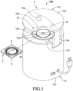
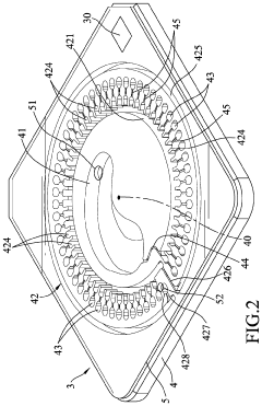
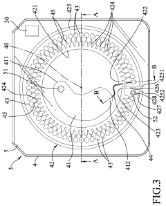
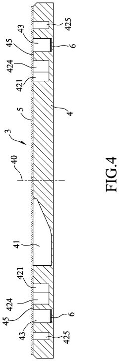
Microfluidic chip and microscopic image system
PatentInactiveUS20200306755A1
Innovation
- A microfluidic chip with a unique structure for precise sample distribution and an automated microscopic image system that includes a machine case assembly with a focus adjusting module and image capture device, allowing for precise image capture and reduced human error.
E-petri dishes, devices, and systems
PatentActiveUS20120223217A1
Innovation
- The e-Petri system employs a CMOS imaging sensor with a transparent layer and a smartphone as an illumination source to capture sub-pixel shifted projection images from different angles, using a processor to reconstruct high-resolution images of specimens, including confluent cell cultures, without the need for mechanical scanning or microfluidic flow.
Materials Science Advancements for Microfluidic Chips
The evolution of microfluidic chip materials represents a critical advancement pathway for high-resolution imaging applications. Traditional materials such as polydimethylsiloxane (PDMS) and glass have dominated the field due to their optical transparency and relatively straightforward fabrication processes. However, these materials present limitations in terms of chemical compatibility, surface properties, and integration capabilities that restrict their performance in advanced imaging scenarios.
Recent developments in materials science have introduced novel substrates that significantly enhance microfluidic imaging capabilities. Cyclic olefin copolymer (COC) and cyclic olefin polymer (COP) have emerged as superior alternatives due to their exceptional optical clarity, low autofluorescence, and minimal water absorption properties. These characteristics make them particularly valuable for fluorescence-based imaging techniques where signal-to-noise ratio is paramount.
Nanomaterial integration represents another frontier in microfluidic chip development. The incorporation of quantum dots, carbon nanotubes, and metallic nanoparticles into chip substrates has enabled enhanced contrast mechanisms and sensing capabilities. Surface plasmon resonance effects from gold nanostructures, for instance, have facilitated super-resolution imaging beyond the diffraction limit when integrated into microfluidic platforms.
Hybrid material systems combining organic and inorganic components have addressed previous limitations in mechanical stability and optical performance. Silicon-glass hybrid chips provide excellent thermal conductivity and dimensional stability while maintaining optical access, critical for temperature-sensitive high-resolution imaging applications. Meanwhile, paper-based microfluidics offer cost-effective alternatives for point-of-care imaging diagnostics, though with resolution trade-offs.
Surface modification technologies have revolutionized the interface between microfluidic channels and biological samples. Hydrophilic coatings reduce non-specific binding that can interfere with imaging clarity, while specialized surface chemistries enable selective immobilization of target molecules for enhanced visualization. These advancements have been particularly valuable for single-molecule imaging techniques within microfluidic environments.
Stimuli-responsive materials represent the cutting edge of microfluidic imaging platforms. These "smart" materials change their properties in response to external stimuli such as temperature, pH, or light, enabling dynamic control of fluid behavior during imaging experiments. For example, thermally responsive polymers can facilitate precise sample positioning for high-resolution imaging by altering channel dimensions or surface properties on demand.
The integration of optically active materials directly into microfluidic structures has opened new possibilities for on-chip microscopy. Waveguides, microlenses, and diffractive elements fabricated from specialized polymers or glasses can manipulate light paths within the chip itself, potentially eliminating bulky external optics while maintaining or even enhancing imaging resolution capabilities.
Integration with AI and Machine Learning Technologies
The integration of artificial intelligence and machine learning technologies with microfluidic chip imaging systems represents a transformative advancement in high-resolution imaging applications. These computational approaches significantly enhance the capabilities of microfluidic platforms by automating analysis, improving image quality, and enabling real-time decision making.
Machine learning algorithms have demonstrated remarkable efficacy in processing the vast datasets generated by microfluidic imaging systems. Deep learning networks, particularly convolutional neural networks (CNNs), excel at feature extraction and pattern recognition in microscopy images, allowing for automated identification of cells, particles, and biological structures with accuracy rates exceeding 95% in optimized systems.
Recent developments have focused on implementing edge computing architectures directly within microfluidic imaging platforms. This integration reduces latency and enables real-time analysis, critical for applications such as flow cytometry and dynamic cell monitoring. The miniaturization of AI processing units has made it possible to incorporate neural network accelerators into portable microfluidic devices, expanding their utility in point-of-care diagnostics.
Computer vision algorithms specifically tailored for microfluidic applications have emerged as a specialized field. These algorithms address unique challenges such as fluid dynamics interference, bubble detection, and multi-plane focusing issues that are common in microfluidic imaging. Transfer learning approaches have proven particularly valuable, allowing models trained on general microscopy datasets to be fine-tuned for specific microfluidic applications with minimal additional training data.
Reinforcement learning techniques are being explored for adaptive imaging control, where the system continuously optimizes imaging parameters based on sample characteristics and flow conditions. This creates a feedback loop between the AI system and the microfluidic platform, resulting in dynamic adjustment of focus, illumination, and capture settings to maximize image quality and information content.
The integration of natural language processing with microfluidic imaging systems is enabling more intuitive interfaces, where researchers can query complex datasets using conversational language rather than complex query languages. This democratizes access to sophisticated analysis capabilities and accelerates the extraction of meaningful insights from experimental data.
Federated learning approaches are addressing privacy concerns in clinical applications by allowing AI models to be trained across multiple institutions without sharing sensitive patient data. This collaborative model development is particularly valuable for rare disease diagnostics, where individual institutions may have limited sample sizes but collectively can generate robust diagnostic algorithms.
AI-driven automation of microfluidic chip operation, combined with intelligent image analysis, is moving the field toward fully autonomous experimental platforms capable of hypothesis generation, experimental design, and result interpretation with minimal human intervention.
Unlock deeper insights with Patsnap Eureka Quick Research — get a full tech report to explore trends and direct your research. Try now!
Generate Your Research Report Instantly with AI Agent
Supercharge your innovation with Patsnap Eureka AI Agent Platform!