

Exploring Semiconductor Chiplet Integration for Patented Solutions
OCT 15, 20259 MIN READ
Generate Your Research Report Instantly with AI Agent
PatSnap Eureka helps you evaluate technical feasibility & market potential.
Chiplet Technology Background and Objectives
Chiplet technology represents a paradigm shift in semiconductor design and manufacturing, evolving from the traditional monolithic system-on-chip (SoC) approach to a more modular and flexible architecture. This evolution began in the early 2010s as semiconductor manufacturers faced increasing challenges with Moore's Law, where the economic and technical feasibility of shrinking transistor sizes became progressively more difficult. The concept of disaggregating large, complex chips into smaller, specialized dies (chiplets) that could be manufactured separately and then integrated together emerged as a promising solution.
The historical trajectory of chiplet technology can be traced back to multi-chip modules (MCMs) used in mainframe computers during the 1980s and 1990s. However, modern chiplet technology distinguishes itself through advanced integration techniques, sophisticated interconnect technologies, and standardized interfaces that enable heterogeneous integration across different process nodes, manufacturers, and even chip architectures.
Industry momentum for chiplet adoption has accelerated significantly since 2017, when AMD introduced its Infinity Fabric interconnect technology in its Ryzen processors, demonstrating the commercial viability of chiplet-based designs. Subsequently, Intel, TSMC, Samsung, and other major semiconductor companies have invested heavily in developing their own chiplet technologies and integration methodologies.
The primary technical objectives of chiplet integration include overcoming the limitations of monolithic chip designs, particularly in terms of manufacturing yield, cost efficiency, and design flexibility. By separating complex systems into smaller, more manageable components, manufacturers can optimize each chiplet for its specific function, potentially using different process technologies for different chiplets within the same package.
Another critical objective is establishing standardized interfaces and protocols for chiplet-to-chiplet communication. Initiatives such as the Universal Chiplet Interconnect Express (UCIe) consortium aim to create industry-wide standards that would enable chiplets from different vendors to work seamlessly together, fostering an open ecosystem for chiplet-based designs.
From a strategic perspective, chiplet technology aims to extend the economic viability of semiconductor scaling beyond what would be possible with traditional monolithic approaches. This is particularly important as the industry approaches the physical limits of silicon-based transistors and faces exponentially increasing costs for advanced process nodes.
Looking forward, the technology roadmap for chiplets includes developing more sophisticated packaging technologies, higher bandwidth and more energy-efficient die-to-die interconnects, and advanced thermal management solutions to address the unique challenges posed by heterogeneous integration. The ultimate goal is to enable a "mix-and-match" approach to system design, where chiplets can be combined like building blocks to create highly customized, high-performance computing solutions tailored to specific application requirements.
Market Demand Analysis for Chiplet Integration
The global semiconductor market is witnessing a paradigm shift towards chiplet integration technology, driven by increasing demands for higher performance, lower power consumption, and cost-effective solutions. Market research indicates that the traditional monolithic chip design approach is reaching its physical and economic limits, creating substantial market opportunities for chiplet-based architectures. The compound annual growth rate (CAGR) for chiplet technology is projected to exceed 40% through 2027, significantly outpacing the broader semiconductor industry's growth rate of 5-7%.
This accelerated market demand stems primarily from data centers and high-performance computing sectors, where the need for processing power continues to grow exponentially while facing thermal and power constraints. Cloud service providers are actively seeking chiplet solutions to address these challenges, with major players allocating substantial portions of their semiconductor procurement budgets to chiplet-based products.
Consumer electronics represents another significant market driver, as smartphone and personal computing device manufacturers pursue higher integration density and improved performance-per-watt metrics. The automotive sector is emerging as a rapidly growing market segment for chiplet technology, particularly for advanced driver assistance systems (ADAS) and autonomous driving platforms that require heterogeneous integration of sensors, processors, and memory components.
From a geographical perspective, North America currently leads chiplet technology adoption, followed closely by East Asia. The European market shows strong growth potential, particularly in automotive and industrial applications. China has made chiplet technology a strategic priority in its semiconductor self-sufficiency initiatives, investing heavily in domestic research and development capabilities.
Market analysis reveals that the chiplet ecosystem is still in its early maturity phase, with significant opportunities for standardization and interoperability solutions. The CHIPS Act in the United States and similar initiatives globally are providing substantial funding for advanced packaging technologies, further accelerating market adoption of chiplet integration approaches.
Industry surveys indicate that over 80% of semiconductor design houses are either actively developing chiplet-based products or planning to incorporate chiplet strategies within their product roadmaps. This widespread industry commitment signals strong market confidence in chiplet technology as a fundamental approach for next-generation semiconductor products rather than a transitional solution.
The economic advantages of chiplet integration are compelling market drivers, with potential yield improvements of 25-30% compared to large monolithic designs, significantly reducing manufacturing costs for complex systems-on-chip. Additionally, the ability to mix process nodes within a single package enables optimized price-performance ratios that are increasingly demanded by cost-sensitive market segments.
Current Semiconductor Chiplet Integration Challenges
The semiconductor industry is currently facing significant challenges in chiplet integration, primarily driven by the slowing of Moore's Law and the increasing complexity of monolithic system-on-chip (SoC) designs. Traditional scaling approaches are encountering physical limitations, with diminishing returns on performance improvements and escalating manufacturing costs. This has catalyzed a paradigm shift toward disaggregated architectures where complex systems are built by integrating smaller, specialized chiplets.
A fundamental challenge in chiplet integration is the development of high-bandwidth, energy-efficient interconnect technologies. Current solutions like silicon interposers provide excellent connectivity but at high manufacturing costs, while organic substrates offer cost advantages but with performance limitations. The industry is actively seeking middle-ground solutions that balance performance, power efficiency, and cost-effectiveness.
Die-to-die interfaces present another significant hurdle, with competing standards emerging from different industry players. The lack of standardization creates interoperability issues and fragments the ecosystem, potentially limiting the adoption of chiplet-based designs. Standards like Universal Chiplet Interconnect Express (UCIe) are gaining traction but have yet to achieve universal adoption across the industry.
Thermal management becomes increasingly complex in chiplet designs due to the concentration of high-performance components and the thermal resistance between dies. The heterogeneous nature of chiplet integration, combining different process nodes and technologies, exacerbates these thermal challenges and necessitates innovative cooling solutions.
Testing and yield management represent critical challenges as well. Traditional testing methodologies designed for monolithic chips are insufficient for multi-chiplet systems, where defects in individual chiplets or their interconnections can compromise overall system performance. Known-good-die testing and system-level validation require new approaches and technologies.
Supply chain complexity increases substantially with chiplet integration, requiring coordination among multiple vendors for different chiplets and packaging technologies. This complexity introduces new risks related to intellectual property protection, manufacturing coordination, and quality assurance across the supply chain.
Design tools and methodologies also lag behind the rapid evolution of chiplet technology. Current electronic design automation (EDA) tools are primarily optimized for monolithic chip design rather than multi-chiplet systems, creating a gap in capabilities for system-level optimization, signal integrity analysis, and thermal simulation across chiplet boundaries.
Addressing these challenges requires collaborative efforts across the semiconductor ecosystem, including innovative patented solutions for interconnect technologies, standardized interfaces, advanced thermal management techniques, and next-generation design and testing methodologies.
Current Patented Chiplet Integration Solutions
01 Interconnect technologies for chiplet integration
Various interconnect technologies are employed to enable effective communication between chiplets in semiconductor integration. These include advanced packaging techniques such as silicon interposers, bridge chips, and through-silicon vias (TSVs) that facilitate high-bandwidth, low-latency connections between multiple chiplets. These interconnect solutions address challenges related to signal integrity, power delivery, and thermal management while enabling heterogeneous integration of chiplets manufactured using different process technologies.- Advanced Interconnect Technologies for Chiplet Integration: Various interconnect technologies are being developed to enable efficient chiplet integration in semiconductor devices. These include through-silicon vias (TSVs), micro-bumps, and hybrid bonding techniques that facilitate high-bandwidth, low-latency communication between chiplets. These advanced interconnect methods allow for heterogeneous integration of different semiconductor components while maintaining performance comparable to monolithic designs.
- Thermal Management Solutions for Chiplet Architectures: Effective thermal management is critical in chiplet-based semiconductor designs due to the high power density and heat generation at interconnect points. Solutions include specialized thermal interface materials, integrated heat spreaders, and novel cooling structures designed specifically for multi-chiplet packages. These thermal management approaches help maintain optimal operating temperatures and prevent performance degradation in densely packed chiplet systems.
- Packaging Technologies for Heterogeneous Chiplet Integration: Advanced packaging technologies enable the integration of diverse chiplets manufactured using different process nodes. These include 2.5D and 3D packaging approaches, silicon interposers, and embedded bridge technologies that allow chiplets with varying functions and manufacturing processes to be combined into a single package. Such packaging innovations support the creation of highly customized semiconductor solutions while leveraging the benefits of specialized manufacturing processes for different components.
- Design Methodologies and Tools for Chiplet-Based Systems: Specialized design methodologies and EDA tools are being developed to address the unique challenges of chiplet-based semiconductor systems. These include tools for chiplet interface standardization, system-level optimization, and design partitioning. Such methodologies enable designers to effectively manage the complexity of multi-chiplet systems, optimize performance across chiplet boundaries, and ensure compatibility between components from different sources.
- Testing and Validation Strategies for Chiplet Integration: Novel testing and validation approaches are essential for ensuring reliability in chiplet-based semiconductor devices. These include known-good-die testing before integration, specialized test structures at chiplet interfaces, and system-level validation methodologies. These strategies help identify defects early in the manufacturing process, ensure proper functionality across chiplet boundaries, and verify the performance of the integrated system under various operating conditions.
02 3D stacking and heterogeneous integration
Three-dimensional stacking techniques allow for vertical integration of chiplets, maximizing silicon density while minimizing footprint. This approach enables the combination of disparate semiconductor technologies (heterogeneous integration) such as logic, memory, analog, and RF components manufactured using different process nodes. The 3D stacking methodology addresses challenges related to die-to-die bonding, thermal dissipation, and power distribution while enabling higher performance and functionality in smaller form factors.Expand Specific Solutions03 Design and verification methodologies for chiplet systems
Specialized design and verification methodologies have been developed to address the unique challenges of chiplet-based semiconductor systems. These include partitioning strategies, interface standardization, and system-level optimization techniques that ensure proper functionality across chiplet boundaries. Advanced simulation and testing approaches validate signal integrity, power integrity, and thermal performance across the integrated chiplet system, ensuring reliable operation under various conditions.Expand Specific Solutions04 Standardized interfaces and protocols for chiplet communication
Standardized interfaces and protocols have been developed to facilitate seamless communication between chiplets from different vendors and process technologies. These standards define electrical, physical, and logical specifications for die-to-die interfaces, enabling a modular approach to semiconductor system design. The standardization efforts address challenges related to interoperability, testing, and validation while promoting a more flexible and cost-effective chiplet ecosystem.Expand Specific Solutions05 Manufacturing and assembly techniques for chiplet integration
Advanced manufacturing and assembly techniques have been developed specifically for chiplet integration, including precision die placement, fine-pitch bonding, and novel substrate technologies. These techniques address challenges related to yield management, thermal expansion mismatch, and mechanical stress while enabling high-volume production of chiplet-based systems. Innovations in testing methodologies ensure that individual chiplets and their interconnections meet performance and reliability requirements before and after integration.Expand Specific Solutions
Key Players in Chiplet Integration Ecosystem
The semiconductor chiplet integration market is currently in a growth phase, with increasing adoption driven by the need for advanced packaging solutions to overcome traditional scaling limitations. The market size is expanding rapidly, projected to reach significant value as chiplet technology becomes essential for high-performance computing applications. From a technical maturity perspective, industry leaders like TSMC, Intel, and Samsung Electronics are at the forefront, having developed advanced chiplet integration technologies and patented solutions. AMD has successfully commercialized chiplet architectures in their processors, while IBM and Micron are advancing memory integration techniques. Emerging players like Chipletz are developing specialized chiplet interconnect solutions, while established manufacturers such as GlobalFoundries and SK hynix are expanding their chiplet capabilities to meet growing demand across computing, data center, and AI applications.
Samsung Electronics Co., Ltd.
Technical Solution: Samsung's chiplet integration strategy centers around their I-Cube (Interposer-Cube) technology, which uses silicon interposers to connect multiple chiplets with high-bandwidth microbumps. Their latest I-Cube4 technology extends this approach with enhanced through-silicon via (TSV) designs that improve signal integrity while reducing power consumption. Samsung has also developed their X-Cube technology, which enables true 3D stacking of logic chiplets using hybrid bonding techniques that achieve interconnect pitches below 7 microns. Their approach includes specialized design tools that optimize chiplet placement and routing to minimize latency between critical components. Samsung's Multi-Die-Integration (MDI) packaging platform supports heterogeneous integration of chiplets manufactured on different process nodes, including their advanced 3nm GAA process technology[9]. They've demonstrated working prototypes combining HBM memory chiplets with logic chiplets in a single package, achieving memory bandwidth exceeding 1.2 TB/s while reducing power consumption by up to 40% compared to traditional implementations[10]. Samsung has also developed specialized test methodologies for known-good-die selection that improve overall yield in multi-chiplet packages.
Strengths: Samsung's vertical integration across memory, logic, and manufacturing gives them unique capabilities to optimize complete chiplet-based systems. Their strong position in memory technologies provides advantages for memory-intensive chiplet designs. Weaknesses: Samsung's chiplet technologies have seen less widespread commercial adoption compared to some competitors, potentially indicating challenges in ecosystem development or cost-effectiveness for certain applications.
Taiwan Semiconductor Manufacturing Co., Ltd.
Technical Solution: TSMC's chiplet integration strategy revolves around their advanced packaging technologies, particularly their Integrated Fan-Out (InFO) and System on Integrated Chips (SoIC) platforms. InFO technology enables high-density connections between multiple chiplets without using a traditional substrate, reducing form factor and improving thermal performance. Their SoIC platform uses hybrid bonding technology to achieve extremely fine-pitch interconnects (less than 10 microns) between chiplets, enabling unprecedented bandwidth density of over 1TB/s/mm² while reducing power consumption by up to 30% compared to traditional packaging methods[3]. TSMC's 3DFabric architecture integrates these technologies with their frontend manufacturing processes, creating a comprehensive platform for heterogeneous integration. Their CoWoS (Chip on Wafer on Substrate) technology has been widely adopted for high-performance computing applications, allowing integration of HBM memory with compute chiplets. TSMC has demonstrated working 3nm chiplets connected via their SoIC technology, showcasing their ability to integrate cutting-edge process nodes with advanced packaging[4].
Strengths: TSMC's industry-leading process technology gives them unique advantages in creating high-performance chiplets. Their broad customer base allows them to develop packaging solutions that address diverse application needs. Weaknesses: As a foundry, TSMC must balance the needs of competing customers, potentially limiting how much they can customize their chiplet solutions for any single client. Their technologies also tend to command premium pricing.
Core Intellectual Property Analysis in Chiplet Technology
Semiconductor chiplet device
PatentActiveUS12230578B2
Innovation
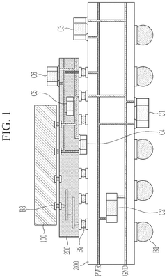
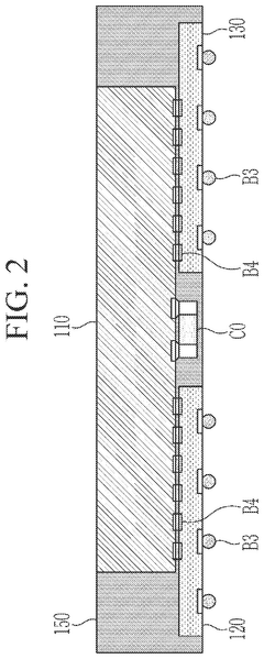
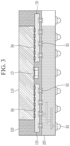
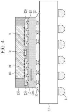
- The semiconductor chiplet device incorporates an interposer layer with at least one decoupling capacitor arranged between the interfaces of the first and second dies, or in the vertical projection area of these interfaces on the package substrate, to form a discharge path that eliminates noise and maintains power integrity.


Semiconductor package with decoupling capacitor and method for manufacturing the same
PatentPendingUS20240332270A1
Innovation
- The implementation of chiplet technology to divide the semiconductor die into multiple dies, allowing for the placement of decoupling capacitors between these dies, ensuring they are closer to the active elements without reducing the number of input/output paths, and using hybrid bonding or solder bumps for connections.
Standardization Efforts in Chiplet Interfaces
The standardization of chiplet interfaces represents a critical foundation for the advancement of heterogeneous integration in semiconductor manufacturing. Industry consortia such as the Universal Chiplet Interconnect Express (UCIe) have emerged as pivotal forces in establishing common protocols for die-to-die communication. UCIe, backed by industry giants including Intel, AMD, Arm, and TSMC, focuses on standardizing physical layer, protocol stack, and software interfaces to ensure interoperability between chiplets from different vendors.
Parallel to UCIe, the Open Compute Project's Bunch of Wires (BoW) interface provides an alternative approach with emphasis on simplicity and cost-effectiveness for chiplet integration. These competing standards highlight the industry's recognition that proprietary interfaces limit the potential of chiplet technology in creating truly modular semiconductor solutions.
The Chiplet Design Exchange (CDX) initiative further complements these efforts by addressing the standardization of design methodologies and verification processes. This framework aims to streamline the integration of chiplets from diverse sources, reducing time-to-market and engineering overhead while maintaining reliability standards.
JEDEC and IEEE have also contributed significantly to chiplet standardization through working groups focused on memory interfaces and high-speed serial links between dies. Their work on HBM (High Bandwidth Memory) interfaces and die-to-die PHY specifications has been instrumental in enabling efficient memory subsystem integration in chiplet-based designs.
Patent landscapes surrounding these standardization efforts reveal strategic positioning by key players. Companies are actively filing patents that both contribute to standards and carve out protected implementation spaces. Notable patent clusters focus on thermal management between chiplets, signal integrity preservation across interfaces, and power delivery optimization in multi-die packages.
The evolution of these standards faces technical challenges including signal integrity at increasing data rates, power efficiency concerns, and thermal management complexities. Testing and validation methodologies for multi-vendor chiplet systems remain underdeveloped, presenting opportunities for innovation in this space.
Future standardization efforts are likely to address emerging needs in chiplet security, authentication mechanisms between dies from different vendors, and advanced power management protocols. The industry is moving toward a "chiplet marketplace" model where standardized interfaces will enable semiconductor components to be mixed and matched like electronic building blocks, fundamentally transforming the semiconductor value chain.
IP Licensing Models and Patent Strategy
In the rapidly evolving semiconductor chiplet ecosystem, intellectual property (IP) licensing models and patent strategies have become critical components for market success. The traditional monolithic IP licensing approach is gradually shifting towards more flexible models that accommodate the distributed nature of chiplet-based designs. Companies are increasingly adopting package-level licensing frameworks where IP rights are negotiated for the entire multi-die package rather than individual components, creating new revenue streams while reducing integration complexities.
Cross-licensing agreements have emerged as a dominant strategy in the chiplet space, allowing companies to access essential technologies without developing everything in-house. These agreements typically include provisions for chiplet interface standards, die-to-die communication protocols, and packaging technologies. Notable examples include AMD's cross-licensing with Intel for x86 architecture while developing proprietary chiplet interconnect technologies.
Patent pools specifically focused on chiplet integration standards are gaining traction, with organizations like CHIPS Alliance and Universal Chiplet Interconnect Express (UCIe) consortium establishing shared IP frameworks. These collaborative models enable broader industry adoption while ensuring fair compensation for innovation contributors. The UCIe consortium, backed by industry giants including Intel, AMD, Arm, and TSMC, represents a significant shift toward standardized licensing approaches for chiplet interfaces.
Defensive patenting has become increasingly important as companies seek to protect their chiplet integration methodologies. Strategic patent filings now focus on interface technologies, thermal management solutions, and testing methodologies specific to multi-die packages. Companies are building comprehensive patent portfolios covering the entire chiplet integration process from design to manufacturing and testing.
Tiered licensing structures are emerging to accommodate different market segments, with premium tiers offering advanced features like enhanced security, higher bandwidth connections, or optimized power management. This approach allows technology providers to serve both high-performance computing markets and cost-sensitive consumer applications with appropriately scaled solutions and licensing costs.
Open-source licensing models are also gaining ground in specific chiplet domains, particularly for standardized interfaces and verification tools. The RISC-V ecosystem demonstrates how open-source IP can accelerate innovation while allowing companies to build proprietary extensions. This hybrid approach balances open collaboration with protected commercial interests, particularly valuable for emerging players seeking to establish presence in the chiplet market.
Unlock deeper insights with PatSnap Eureka Quick Research — get a full tech report to explore trends and direct your research. Try now!
Generate Your Research Report Instantly with AI Agent
Supercharge your innovation with PatSnap Eureka AI Agent Platform!