Exploring the Regulatory Landscape for Chiplet Integration
OCT 15, 202510 MIN READ
Generate Your Research Report Instantly with AI Agent
PatSnap Eureka helps you evaluate technical feasibility & market potential.
Chiplet Integration Regulatory Background and Objectives
Chiplet integration technology has evolved significantly over the past decade as a response to the slowing of Moore's Law and increasing challenges in traditional monolithic chip design. This architectural approach, which involves integrating multiple smaller silicon dies (chiplets) into a single package, emerged as semiconductor manufacturers faced physical limitations in scaling transistors below 10nm. The regulatory landscape surrounding chiplet integration has been shaped by both technical necessities and market demands, with initial frameworks appearing around 2015-2017 when companies like AMD and Intel began commercializing multi-die packages.
The regulatory environment for chiplet integration spans multiple domains including intellectual property protection, standardization efforts, international trade regulations, and security considerations. Early regulatory approaches were largely fragmented, with individual companies developing proprietary interconnect technologies and packaging methods. This created significant barriers to the broader adoption of chiplet-based designs and limited interoperability between chiplets from different manufacturers.
A pivotal development occurred in 2019 with the formation of the Universal Chiplet Interconnect Express (UCIe) consortium, which aimed to establish industry-wide standards for chiplet interfaces. This marked a shift toward collaborative regulatory frameworks designed to enable an open chiplet ecosystem. Concurrently, government entities in major semiconductor manufacturing regions began developing policies to address the strategic importance of advanced packaging technologies, including chiplet integration.
The primary objectives of current regulatory efforts focus on several key areas. First is establishing standardized interfaces and protocols to enable chiplet interoperability across vendors, which is crucial for creating a competitive marketplace. Second is addressing intellectual property concerns through licensing frameworks that balance innovation protection with ecosystem growth. Third is developing security standards specific to multi-die architectures, which present unique attack surfaces compared to monolithic designs.
Additionally, regulatory frameworks aim to navigate the complex geopolitical landscape affecting semiconductor supply chains. With chiplet integration enabling more distributed manufacturing models, regulations must address concerns about technology transfer, export controls, and supply chain resilience. This is particularly relevant as chiplet technology allows for the separation of design and manufacturing across different geographical regions and companies.
The technical goals of regulatory development include defining testing and validation methodologies specific to chiplet-based systems, establishing thermal and power management standards, and creating certification processes that ensure reliability across heterogeneous integration approaches. These efforts are essential for chiplet technology to achieve mainstream adoption across diverse application domains from high-performance computing to edge devices.
Market Demand Analysis for Chiplet Technology
The global chiplet market is experiencing unprecedented growth, driven by the increasing demand for high-performance computing solutions across various industries. Current market projections indicate that the chiplet technology market is expected to grow at a compound annual growth rate of over 40% from 2023 to 2030, reaching significant market valuation by the end of the decade. This remarkable growth trajectory is primarily fueled by the semiconductor industry's shift away from traditional monolithic designs toward more modular and efficient chiplet-based architectures.
The demand for chiplet technology is particularly strong in data centers and cloud computing environments, where the need for processing power continues to escalate due to artificial intelligence, machine learning, and big data applications. These computational workloads require increasingly powerful processors that traditional monolithic designs struggle to deliver efficiently. Chiplet-based solutions offer improved performance, power efficiency, and cost-effectiveness, making them highly attractive for these demanding applications.
Consumer electronics represents another significant market segment driving chiplet adoption. As smartphones, tablets, and other personal devices incorporate more advanced features like on-device AI processing and augmented reality capabilities, the demand for more powerful yet energy-efficient processors grows. Chiplet technology enables device manufacturers to create customized solutions that balance performance and power consumption according to specific product requirements.
Automotive and industrial sectors are emerging as promising markets for chiplet technology. Advanced driver-assistance systems (ADAS), autonomous vehicles, and industrial automation require sophisticated computing capabilities that can operate reliably in challenging environments. Chiplet-based designs offer the flexibility and performance needed for these applications while potentially reducing costs through more efficient manufacturing processes.
The market demand for chiplet technology is further accelerated by the slowing of Moore's Law and the increasing challenges in traditional semiconductor scaling. As process node advancements become more difficult and expensive, chiplet architecture provides an alternative path to continued performance improvements. This approach allows manufacturers to combine the best features of different process nodes and specialized technologies, creating heterogeneous integrated systems that outperform conventional monolithic designs.
Geographically, North America and Asia-Pacific regions dominate the chiplet market, with major semiconductor companies and foundries investing heavily in research and development. However, Europe is also making significant strides in chiplet technology development, particularly in automotive and industrial applications, creating a truly global market landscape for this emerging technology.
Global Regulatory Status and Technical Challenges
The global regulatory landscape for chiplet integration remains fragmented, with different regions adopting varying approaches to standardization and compliance requirements. In the United States, the Department of Commerce has begun developing preliminary frameworks for chiplet interoperability standards, though these remain largely voluntary. The National Institute of Standards and Technology (NIST) has established working groups focused specifically on chiplet interface protocols and testing methodologies, aiming to create reference architectures that could eventually become regulatory benchmarks.
The European Union has taken a more structured approach through its European Chips Act, which explicitly addresses heterogeneous integration technologies including chiplets. The EU's regulatory framework emphasizes security validation and certification processes for critical infrastructure applications, creating additional compliance hurdles for chiplet-based systems intended for deployment in sensitive sectors such as telecommunications and defense.
In Asia, regulatory approaches vary significantly by country. Japan's Ministry of Economy, Trade and Industry has established technical committees focused on chiplet standardization with particular emphasis on thermal management and reliability testing protocols. South Korea has integrated chiplet technology considerations into its K-Semiconductor Belt strategy, with government-backed certification programs for multi-die packages. China, meanwhile, has accelerated development of its own chiplet standards through the China Electronics Standardization Institute, potentially creating regional interoperability challenges.
Technical challenges accompanying these regulatory developments are substantial. The lack of globally harmonized standards for chiplet interfaces presents significant obstacles for international supply chains. Die-to-die interconnect protocols remain particularly problematic, with competing standards including Universal Chiplet Interconnect Express (UCIe), Advanced Interface Bus (AIB), and Bunch of Wires (BoW) each gaining regional regulatory preference without clear global consensus.
Testing and validation methodologies represent another critical regulatory challenge. Current regulatory frameworks struggle to address known-good-die verification in heterogeneous integration scenarios, creating uncertainty around liability and certification requirements. The complexity of thermal and power integrity validation across multiple chiplets further complicates regulatory compliance, with few standardized methodologies available.
Security certification presents perhaps the most significant regulatory hurdle. Multiple jurisdictions have begun implementing chiplet-specific security requirements, particularly for applications in critical infrastructure. These include enhanced side-channel attack resistance validation and hardware root-of-trust verification across die boundaries. The fragmented nature of these security requirements creates substantial compliance challenges for global chiplet deployment.
Current Regulatory Compliance Solutions
01 Advanced Interconnect Technologies for Chiplet Integration
Various interconnect technologies are being developed to enable efficient chiplet integration. These include advanced packaging methods, through-silicon vias (TSVs), and high-density interconnects that facilitate communication between different chiplets. These technologies aim to minimize signal delay, reduce power consumption, and enhance overall system performance by optimizing the connections between integrated chiplets.- Advanced Packaging Technologies for Chiplet Integration: Advanced packaging technologies are essential for chiplet integration, enabling multiple dies to be combined into a single package. These technologies include 2.5D and 3D integration methods, interposer-based solutions, and fan-out wafer-level packaging. These approaches allow for heterogeneous integration of chiplets with different functionalities, process nodes, or from different manufacturers, while maintaining high performance interconnections between the dies.
- Interconnect Technologies for Chiplet Communication: Interconnect technologies are crucial for enabling efficient communication between chiplets in an integrated system. These include high-bandwidth die-to-die interfaces, through-silicon vias (TSVs), micro-bumps, and advanced redistribution layers. The interconnect solutions must provide high data transfer rates, low latency, and minimal power consumption while maintaining signal integrity across the chiplet boundaries.
- Thermal Management Solutions for Chiplet Designs: Thermal management is a critical aspect of chiplet integration as the dense packaging of multiple dies can lead to significant heat generation. Solutions include integrated heat spreaders, thermal interface materials, embedded cooling channels, and advanced heat dissipation structures. Effective thermal management ensures optimal performance and reliability of chiplet-based systems by preventing thermal throttling and reducing the risk of thermal-induced failures.
- Design and Testing Methodologies for Chiplet-Based Systems: Specialized design and testing methodologies are required for chiplet-based systems to ensure functionality and reliability. These include modular design approaches, known-good-die testing strategies, design-for-test features specific to chiplet architectures, and standardized interfaces. These methodologies address the unique challenges of integrating pre-tested chiplets from potentially different sources while maintaining system-level performance and yield.
- Standardization and Ecosystem Development for Chiplet Integration: Standardization efforts and ecosystem development are essential for widespread adoption of chiplet integration. This includes the development of common interfaces, protocols, and design standards that enable interoperability between chiplets from different vendors. Industry consortia are working to establish specifications for physical interfaces, power delivery, and communication protocols to create an open chiplet ecosystem that reduces design complexity and time-to-market for chiplet-based products.
02 Thermal Management Solutions for Chiplet Architectures
Effective thermal management is crucial for chiplet-based systems due to the high power density and heat generation. Various cooling solutions are being implemented, including integrated heat spreaders, thermal interface materials, and advanced cooling mechanisms. These solutions help maintain optimal operating temperatures, prevent thermal throttling, and ensure reliable performance of multi-chiplet systems.Expand Specific Solutions03 Heterogeneous Integration of Chiplets
Heterogeneous integration involves combining chiplets manufactured using different process technologies or having different functionalities into a single package. This approach allows for optimizing each component separately while maintaining system-level integration. It enables the combination of high-performance logic, memory, analog, and specialized accelerators in a modular fashion, leading to improved performance, power efficiency, and cost-effectiveness.Expand Specific Solutions04 Design and Testing Methodologies for Chiplet-Based Systems
Specialized design and testing methodologies are being developed for chiplet-based systems. These include design-for-test approaches, pre-bond and post-bond testing strategies, and verification techniques specific to multi-die integration. Advanced tools and methodologies help ensure functionality, reliability, and yield improvement in complex chiplet architectures, addressing challenges related to inter-chiplet communication and system-level validation.Expand Specific Solutions05 Packaging Technologies for Chiplet Integration
Advanced packaging technologies are essential for successful chiplet integration. These include 2.5D and 3D packaging approaches, silicon interposers, organic substrates, and fan-out wafer-level packaging. These technologies provide the physical platform for integrating multiple chiplets while addressing challenges related to power delivery, signal integrity, and mechanical stability, enabling higher performance and more compact system designs.Expand Specific Solutions
Key Industry Players and Ecosystem Analysis
The chiplet integration regulatory landscape is evolving rapidly as the semiconductor industry transitions from traditional monolithic designs to modular approaches. Currently in the early growth phase, this market is expanding significantly due to increasing demand for specialized computing solutions. While established players like TSMC, Intel, and AMD lead with mature chiplet technologies, newer entrants including GlobalFoundries and Micron are developing competitive offerings. The ecosystem is characterized by varying levels of technical maturity, with companies like IBM and Samsung focusing on standardization efforts, while others like Huawei and Google are investing in proprietary integration methodologies. Regulatory frameworks remain fragmented globally, creating compliance challenges as chiplet technology crosses traditional semiconductor boundaries.
GLOBALFOUNDRIES, Inc.
Technical Solution: GLOBALFOUNDRIES has developed a specialized approach to chiplet integration focused on addressing the regulatory challenges in sensitive markets like aerospace, defense, and automotive. Their 22FDX platform provides a foundation for chiplet-based designs with specific features to meet regulatory requirements for reliability and longevity. GF has established a Trusted Foundry program that complies with US government security regulations, allowing them to manufacture chiplets for applications with strict regulatory oversight. Their approach includes implementing secure manufacturing protocols that maintain the chain of custody throughout the chiplet production process, addressing regulatory concerns about supply chain security. GF works closely with standards organizations like the Automotive Electronics Council to ensure their chiplet manufacturing processes meet industry-specific regulatory requirements. The company has developed specialized testing methodologies for chiplets that comply with various international standards, including those for radiation hardness in aerospace applications and functional safety in automotive systems according to ISO 26262.
Strengths: Specialized expertise in regulated industries; established trusted manufacturing capabilities; strong presence in both US and European regulatory environments. Weaknesses: More limited advanced node capabilities compared to TSMC; focused on specific market segments rather than broad consumer applications.
Taiwan Semiconductor Manufacturing Co., Ltd.
Technical Solution: TSMC has developed an advanced chiplet integration platform called 3DFabric, which addresses regulatory challenges through a comprehensive approach to heterogeneous integration. Their solution encompasses front-end and back-end technologies including TSMC-SoIC (System on Integrated Chips), CoWoS (Chip on Wafer on Substrate), and InFO (Integrated Fan-Out) packaging. TSMC has established a dedicated regulatory compliance framework for their chiplet technologies that addresses export control regulations, particularly navigating the complex US-China trade restrictions. Their approach includes implementing secure supply chain protocols and traceability systems that meet international standards for semiconductor manufacturing. TSMC works closely with standards organizations like SEMI and IEEE to develop industry-wide specifications for chiplet interfaces and testing methodologies. Their advanced packaging facilities are certified to meet regulatory requirements across multiple jurisdictions, with particular attention to environmental regulations regarding chemical usage and waste management in the packaging process.
Strengths: World-leading manufacturing capabilities with established regulatory compliance systems; comprehensive portfolio of integration technologies; strong relationships with global regulatory bodies. Weaknesses: Caught in geopolitical tensions affecting technology transfer regulations; limited control over end-use applications of their chiplet technologies.
Critical Patents and Standards for Chiplet Integration
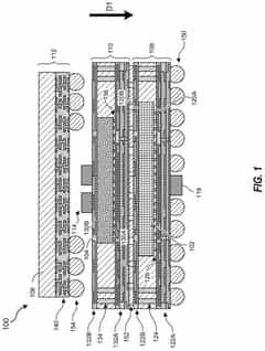
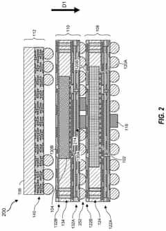
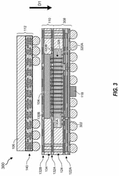
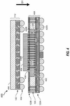
3D chiplet integration using fan-out wafer-level packaging
PatentPendingUS20240274587A1
Innovation
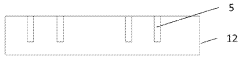
- The use of fan-out wafer-level packaging and three-dimensional packaging techniques for combining semiconductor chips and embedded memory in configurations such as face-to-back, back-to-back, and face-to-face orientations, enabling direct connections between chiplets and reducing assembly package sizes and manufacturing complexity.
Integrated structure and integration method suitable for wafer-scale heterogeneous chiplet
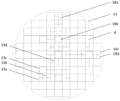
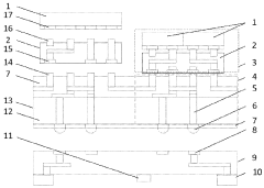
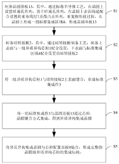
PatentWO2024011880A1
Innovation
- 通过在晶圆基板上设置硅通孔阵列和重复的标准集成区域,并制备具有异构转接板微凸点和微焊盘的硅转接板,形成标准集成件,实现异质异构芯粒与晶圆基板的键合,利用多层重布线层实现芯粒间的互通连接。
Cross-Border Compliance Framework
The global regulatory landscape for chiplet integration presents a complex matrix of compliance requirements that vary significantly across jurisdictions. Companies operating in the chiplet ecosystem must navigate a multifaceted framework of regulations spanning intellectual property protection, data security, export controls, and technical standards. These regulations often reflect national security interests and industrial policies rather than purely technical considerations.
In the United States, the Bureau of Industry and Security (BIS) has implemented export controls specifically targeting advanced semiconductor technologies, including those related to chiplet integration. These controls restrict the transfer of certain technologies to designated countries and entities, requiring manufacturers to obtain licenses for cross-border chiplet supply chains. Similarly, the European Union has established the European Chips Act, which includes provisions for security certification of integrated circuits and systems, directly impacting chiplet-based designs.
Asian regulatory frameworks present additional complexity. Japan's Ministry of Economy, Trade and Industry (METI) has strengthened its export control regime for semiconductor technologies, while South Korea has implemented the Act on Prevention of Divulgence and Protection of Industrial Technology. China's regulatory approach includes both the Cybersecurity Law and Export Control Law, which together create significant compliance hurdles for international chiplet integration projects involving Chinese entities.
Technical standards compliance adds another layer to the regulatory framework. Organizations such as IEEE, JEDEC, and the Universal Chiplet Interconnect Express (UCIe) consortium have developed standards that, while technically voluntary, often become de facto regulatory requirements for market access. These standards address interoperability, testing methodologies, and performance benchmarks that chiplet designs must meet.
Data sovereignty regulations present particular challenges for chiplet integration. The cross-border flow of design data, testing parameters, and intellectual property must comply with regulations such as the EU's General Data Protection Regulation (GDPR) and China's Personal Information Protection Law (PIPL), even when the data relates to technical specifications rather than personal information.
Intellectual property protection frameworks vary substantially across jurisdictions, creating compliance challenges for chiplet designers who must navigate different patent systems, trade secret protections, and licensing requirements. The fragmentation of IP rights across multiple countries can create significant legal uncertainty for global chiplet supply chains.
Companies pursuing chiplet integration strategies must implement comprehensive compliance programs that address this regulatory complexity. These programs typically include jurisdiction-specific risk assessments, technical controls to prevent unauthorized technology transfers, and contractual frameworks that allocate compliance responsibilities across the supply chain.
Intellectual Property Protection Strategies
In the rapidly evolving landscape of chiplet integration, intellectual property (IP) protection has emerged as a critical concern for industry stakeholders. As chiplet technology enables the disaggregation of monolithic systems into smaller functional blocks, companies must develop robust strategies to safeguard their innovations while navigating complex cross-licensing scenarios.
Patent portfolios represent the cornerstone of IP protection for chiplet technologies. Organizations should pursue comprehensive patent coverage across multiple dimensions: interface standards, integration methodologies, testing protocols, and thermal management solutions. Strategic patent filing in key jurisdictions—particularly the United States, China, Taiwan, and the European Union—provides essential territorial protection where chiplet manufacturing and integration predominantly occur.
Trade secret protection offers complementary coverage for aspects of chiplet technology that may not be readily discernible through reverse engineering. This includes proprietary manufacturing processes, specialized testing methodologies, and optimization algorithms. Companies should implement rigorous internal controls, including employee confidentiality agreements, access restrictions, and compartmentalized information sharing protocols to maintain trade secret status.
The standardization of chiplet interfaces presents unique IP challenges. Companies must balance participation in open standards development with protection of proprietary innovations. Strategic approaches include contributing essential patents to standards while maintaining differentiated IP around implementation details, or developing a two-tier approach with standardized external interfaces and proprietary internal architectures.
Cross-licensing agreements have become increasingly important in the chiplet ecosystem. These arrangements enable technology sharing while reducing litigation risks. Companies should develop tiered licensing strategies that distinguish between core and peripheral technologies, with corresponding differentiated royalty structures. Defensive patent aggregation through industry consortia can also provide collective protection against non-practicing entities.
Open-source strategies are gaining traction for certain chiplet technologies. Selective open-sourcing of interface specifications while maintaining proprietary implementation details can accelerate adoption while preserving competitive advantages. This approach requires careful IP segmentation and clear licensing terms to prevent unintended technology transfer.
For emerging players, IP acquisition strategies—including targeted acquisitions of startups with complementary chiplet technologies or licensing arrangements with established IP holders—can rapidly build defensive portfolios. These strategies must be balanced against cost considerations and alignment with long-term technology roadmaps.
Unlock deeper insights with PatSnap Eureka Quick Research — get a full tech report to explore trends and direct your research. Try now!
Generate Your Research Report Instantly with AI Agent
Supercharge your innovation with PatSnap Eureka AI Agent Platform!