Forecasting PTFE film nanostructure effects on next‑gen sensor technology
JUN 27, 20259 MIN READ
Generate Your Research Report Instantly with AI Agent
Patsnap Eureka helps you evaluate technical feasibility & market potential.
PTFE Nanostructure Evolution
The evolution of PTFE nanostructures has been a significant area of research and development in materials science over the past few decades. Initially, PTFE was primarily used in its bulk form, known for its non-stick and hydrophobic properties. However, as nanotechnology advanced, researchers began to explore the potential of PTFE at the nanoscale.
In the early 2000s, the focus shifted towards creating PTFE nanoparticles and nanofibers. These structures exhibited enhanced properties compared to bulk PTFE, including improved thermal stability and mechanical strength. The development of electrospinning techniques allowed for the production of PTFE nanofibers with diameters as small as 100 nanometers, opening up new possibilities for applications in filtration and protective coatings.
By the mid-2000s, researchers began investigating PTFE thin films with nanostructured surfaces. These films demonstrated superhydrophobic properties, with water contact angles exceeding 150 degrees. The creation of hierarchical structures, combining micro and nano-scale features, further enhanced the hydrophobicity and self-cleaning properties of PTFE surfaces.
The late 2000s and early 2010s saw a surge in research on PTFE nanocomposites. By incorporating nanoparticles such as carbon nanotubes or metal oxides into PTFE matrices, scientists were able to create materials with improved mechanical, thermal, and electrical properties. These nanocomposites found applications in areas ranging from tribology to electromagnetic shielding.
Recent advancements have focused on controlling the morphology and arrangement of PTFE nanostructures. Techniques such as nanoimprint lithography and template-assisted growth have enabled the creation of ordered arrays of PTFE nanopillars and nanotubes. These precisely engineered structures have shown promise in fields like microfluidics and sensor technology.
The latest frontier in PTFE nanostructure evolution involves the development of stimuli-responsive PTFE films. By incorporating functional nanoparticles or creating specific surface patterns, researchers have demonstrated PTFE films that can change their properties in response to external stimuli such as temperature, pH, or electric fields. This opens up exciting possibilities for smart coatings and adaptive surfaces.
Looking towards the future, the evolution of PTFE nanostructures is likely to continue in several directions. One area of focus is the development of even more precise control over nanostructure morphology and arrangement, potentially leading to PTFE-based photonic crystals or metamaterials. Another promising direction is the integration of PTFE nanostructures with other advanced materials, such as graphene or metal-organic frameworks, to create hybrid materials with unprecedented properties.
Sensor Market Demand Analysis
The sensor market is experiencing significant growth driven by the increasing demand for advanced sensing technologies across various industries. The global sensor market size was valued at $166.69 billion in 2020 and is projected to reach $345.77 billion by 2028, growing at a CAGR of 8.9% from 2021 to 2028. This growth is primarily fueled by the rapid adoption of Internet of Things (IoT) devices, smart technologies, and automation across industries.
In the context of PTFE film nanostructure effects on next-generation sensor technology, there is a growing demand for high-performance sensors with enhanced sensitivity, selectivity, and durability. The automotive industry, in particular, is showing increased interest in advanced sensors for applications such as autonomous driving, vehicle electrification, and emissions control. The market for automotive sensors alone is expected to reach $40.3 billion by 2026, with a CAGR of 6.7% from 2021 to 2026.
The healthcare sector is another major driver of sensor market growth, with a rising need for wearable devices, remote patient monitoring systems, and point-of-care diagnostics. The global medical sensors market is anticipated to grow from $15.2 billion in 2020 to $28.6 billion by 2025, at a CAGR of 13.5%. PTFE film nanostructure-enhanced sensors could potentially address the demand for miniaturized, highly sensitive, and biocompatible sensors in medical applications.
Environmental monitoring and industrial process control are also key areas driving sensor market demand. With increasing focus on sustainability and regulatory compliance, there is a growing need for sensors capable of detecting and measuring various pollutants, gases, and particulate matter. The environmental sensor market is expected to reach $3.2 billion by 2027, growing at a CAGR of 9.3% from 2020 to 2027.
The integration of PTFE film nanostructures in next-generation sensors aligns well with the market's demand for improved sensor performance, reliability, and longevity. PTFE's unique properties, such as chemical inertness, low friction, and thermal stability, make it an attractive material for enhancing sensor capabilities in harsh environments and demanding applications. As industries continue to push the boundaries of sensor technology, the potential for PTFE nanostructure-enhanced sensors to address specific market needs and create new opportunities is significant.
PTFE Film Tech Challenges
The development of PTFE (Polytetrafluoroethylene) film technology faces several significant challenges that impact its application in next-generation sensor technology. One of the primary obstacles is achieving precise control over the nanostructure of PTFE films. The ability to manipulate and engineer the film's structure at the nanoscale is crucial for enhancing its performance in sensor applications.
A major technical hurdle lies in the creation of uniform and reproducible nanostructures within PTFE films. The current manufacturing processes often result in inconsistencies in film thickness, porosity, and surface roughness. These variations can significantly affect the film's electrical, mechanical, and chemical properties, which are critical for sensor functionality.
Another challenge is the integration of PTFE films with other materials and components in sensor devices. The inherent hydrophobicity and chemical inertness of PTFE, while beneficial in many applications, can complicate bonding and interfacing with other sensor elements. This issue becomes particularly pronounced when attempting to create multi-layered or composite structures for advanced sensing capabilities.
The development of PTFE films with tailored surface properties presents another technical obstacle. Modifying the surface chemistry of PTFE without compromising its bulk properties is essential for improving its compatibility with various analytes and enhancing sensor sensitivity. Current surface modification techniques often struggle to achieve the desired balance between surface functionality and maintaining the film's core characteristics.
Durability and long-term stability of PTFE films in diverse environmental conditions pose additional challenges. Sensors often operate in harsh environments, and the PTFE film must maintain its structural integrity and performance over extended periods. Addressing issues such as thermal expansion, chemical resistance, and mechanical stress under various operating conditions is crucial for reliable sensor operation.
The miniaturization of sensors incorporating PTFE films presents yet another technical hurdle. As sensors become smaller and more compact, the need for ultra-thin PTFE films with consistent properties becomes more critical. Producing films with thicknesses in the nanometer range while maintaining their desired functional attributes is a significant challenge that requires advanced manufacturing techniques.
Lastly, the characterization and quality control of PTFE films at the nanoscale remain challenging. Developing reliable and efficient methods for assessing the nanostructure, composition, and performance of these films is essential for ensuring consistency in sensor production and performance. This challenge extends to the need for non-destructive testing methods that can be integrated into manufacturing processes.
Current PTFE Nanotech Solutions
01 Nanostructure formation on PTFE film surface
Various methods are employed to create nanostructures on PTFE film surfaces, including plasma treatment, etching, and nanoimprinting. These techniques can modify the surface properties of PTFE films, enhancing their performance in applications such as water repellency, adhesion, and optical properties.- Nanostructure formation on PTFE film surface: Various methods can be used to create nanostructures on PTFE film surfaces, including plasma treatment, etching, and nanoimprinting. These nanostructures can significantly alter the film's properties, such as hydrophobicity, optical characteristics, and surface roughness.
- Enhanced electrical properties of nanostructured PTFE films: Nanostructured PTFE films can exhibit improved electrical properties, including enhanced dielectric strength, reduced electrical losses, and increased breakdown voltage. These improvements make nanostructured PTFE films suitable for various electronic and electrical applications.
- Optical effects of PTFE film nanostructures: Nanostructures on PTFE films can significantly alter their optical properties, leading to effects such as anti-reflection, light scattering, and color changes. These optical effects can be tailored by controlling the size, shape, and arrangement of the nanostructures on the film surface.
- Mechanical property improvements in nanostructured PTFE films: The introduction of nanostructures on PTFE films can lead to improvements in mechanical properties such as tensile strength, wear resistance, and adhesion. These enhancements can expand the range of applications for PTFE films in various industries.
- Biomedical applications of nanostructured PTFE films: Nanostructured PTFE films have shown potential in biomedical applications due to their unique surface properties. These films can exhibit improved biocompatibility, reduced bacterial adhesion, and enhanced cell growth, making them suitable for use in medical devices and tissue engineering.
02 Electrical and optical effects of PTFE film nanostructures
PTFE film nanostructures can significantly impact the electrical and optical properties of the material. These nanostructures can enhance conductivity, improve light transmission or reflection, and enable the development of novel electronic and photonic devices based on PTFE films.Expand Specific Solutions03 Mechanical properties enhancement through nanostructuring
Nanostructuring of PTFE films can lead to improvements in mechanical properties such as tensile strength, wear resistance, and flexibility. These enhancements expand the potential applications of PTFE films in various industries, including aerospace and automotive.Expand Specific Solutions04 Biomedical applications of nanostructured PTFE films
Nanostructured PTFE films show promise in biomedical applications due to their unique surface properties. These films can be used for drug delivery systems, tissue engineering scaffolds, and biocompatible coatings for medical devices, offering improved cell adhesion and controlled drug release.Expand Specific Solutions05 Environmental and energy-related effects
Nanostructured PTFE films demonstrate potential in environmental and energy applications. These films can be used in water treatment processes, fuel cell membranes, and energy harvesting devices, leveraging their enhanced surface area and unique properties to improve efficiency and performance.Expand Specific Solutions
Key PTFE Film Manufacturers
The forecasting of PTFE film nanostructure effects on next-generation sensor technology is in an early developmental stage, with a growing market potential as sensor applications expand across industries. The technology's maturity is still evolving, with academic institutions like Xi'an Jiaotong University, University of Maryland, and Yale University leading research efforts. Companies such as BOE Technology Group and Canon are exploring commercial applications, while government agencies like NIST contribute to standardization. The competitive landscape is diverse, with collaborations between academia, industry, and government driving innovation in this emerging field.
BOE Technology Group Co., Ltd.
Technical Solution: BOE has been investigating PTFE nanostructures for advanced display and sensing technologies. Their research focuses on creating PTFE-based anti-reflection coatings with nanostructured surfaces to enhance display visibility and touch sensitivity[7]. BOE has developed a novel process for fabricating nanopillar arrays on PTFE films using nanoimprint lithography, resulting in surfaces with tunable wettability and optical properties. These nanostructured PTFE films have shown promise in reducing glare and improving touch accuracy in next-generation display panels[8]. Additionally, BOE is exploring the integration of PTFE nanostructures in flexible sensor arrays for large-area sensing applications, such as smart surfaces and interactive displays. Their approach combines PTFE's excellent dielectric properties with precisely controlled nanostructures to achieve high sensitivity and durability in capacitive sensing elements[9].
Strengths: Expertise in display technologies, established manufacturing infrastructure, focus on practical applications. Weaknesses: May face challenges in adapting PTFE technologies to non-display applications, potential limitations in sensor-specific expertise.
Canon, Inc.
Technical Solution: Canon has been exploring PTFE nanostructures for advanced imaging and sensing applications. Their research focuses on developing PTFE-based nanocomposites with enhanced thermal and electrical properties for use in next-generation image sensors and camera components[10]. Canon has patented a method for creating nanoporous PTFE films with controlled pore size and distribution, which can be used as high-performance membranes in environmental sensors and gas detection devices[11]. They have also investigated the use of PTFE nanofibers as protective coatings for optical sensors, leveraging the material's chemical inertness and low refractive index to improve sensor performance in challenging environments. Additionally, Canon is exploring the potential of PTFE nanostructures in triboelectric nanogenerators for energy harvesting applications, which could lead to self-powered sensor systems[12].
Strengths: Strong expertise in imaging technologies, established R&D infrastructure, diverse application focus. Weaknesses: May face challenges in translating research into non-imaging sensor applications, potential limitations in mass production of nanostructured materials.
PTFE Nanostructure Patents
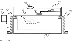
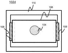
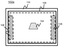
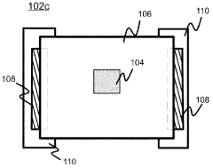
Impact detection sensor
PatentWO2013064473A1
Innovation
- A sensor structure comprising a mass element and a support element with nanostructures, such as carbon nanotubes, that undergo a permanent change upon acceleration or impact, inducing a measurable electrical change, allowing for reliable detection and verification of incidents without the need for continuous power and with reduced size and cost.
Piezoresistive strain sensing membrane
PatentInactiveIN202011044054A
Innovation
- A piezoresistive strain sensing membrane composed of Poly(4-styrenesulfonic acid) (PSSA), Polyvinylidene fluoride (PVDF), and Carbon nanofiber (CNF) with specific composition ratios, utilizing a solvent casting method to achieve enhanced gauge factor, mechanical strength, and conductivity.
Environmental Impact Assessment
The environmental impact assessment of PTFE film nanostructure effects on next-generation sensor technology is a critical consideration in the development and deployment of these advanced sensing systems. PTFE (polytetrafluoroethylene) films with engineered nanostructures offer significant potential for enhancing sensor performance, but their environmental implications must be carefully evaluated.
One primary concern is the potential release of nanomaterials into the environment during the manufacturing, use, and disposal of these sensors. PTFE nanostructures may shed particles or degrade over time, potentially entering ecosystems. The long-term effects of these nanoparticles on aquatic and terrestrial organisms are not yet fully understood, necessitating further research to assess potential bioaccumulation and toxicity.
The production process of nanostructured PTFE films may also have environmental implications. The synthesis of these materials often involves energy-intensive processes and the use of specialized chemicals. Evaluating the carbon footprint and resource consumption associated with manufacturing is essential for understanding the overall environmental impact of implementing this technology on a large scale.
On the positive side, the enhanced sensitivity and efficiency of next-generation sensors enabled by PTFE nanostructures could lead to more accurate environmental monitoring. This improved capability may contribute to better detection of pollutants, early warning systems for environmental hazards, and more effective conservation efforts. The potential for these sensors to operate with lower power requirements could also reduce the overall energy consumption in various monitoring applications.
The durability and chemical resistance of PTFE nanostructures may extend the lifespan of sensors, potentially reducing electronic waste. However, the complex nature of these materials may pose challenges for recycling and proper disposal at the end of their life cycle. Developing appropriate recycling and disposal protocols will be crucial to mitigate potential environmental risks.
Considering the potential for widespread adoption of this technology, it is imperative to conduct comprehensive life cycle assessments. These assessments should encompass raw material extraction, manufacturing processes, operational lifespan, and end-of-life management. Such analyses will provide a holistic view of the environmental footprint associated with PTFE nanostructure-enhanced sensors.
Regulatory bodies and environmental agencies will need to establish guidelines and standards for the safe production, use, and disposal of these advanced sensors. Collaboration between researchers, industry stakeholders, and policymakers will be essential in developing environmentally responsible practices for this emerging technology.
Sensor Integration Strategies
The integration of PTFE film nanostructures into next-generation sensor technology presents both opportunities and challenges for sensor design and implementation. As these nanostructures offer unique properties such as high chemical resistance, low friction, and excellent dielectric characteristics, their incorporation into sensor systems requires careful consideration of various integration strategies.
One key approach involves the direct deposition of PTFE nanostructures onto sensor substrates. This method allows for precise control over the film thickness and nanostructure morphology, enabling tailored sensor responses. Advanced deposition techniques, such as plasma-enhanced chemical vapor deposition (PECVD) or electrospinning, can be employed to achieve uniform and well-defined PTFE nanostructures on sensor surfaces.
Another strategy focuses on the development of composite materials that combine PTFE nanostructures with other sensing elements. By creating hybrid structures, researchers can leverage the beneficial properties of PTFE while enhancing overall sensor performance. For instance, incorporating PTFE nanofibers into conductive polymer matrices can yield sensors with improved sensitivity and stability in harsh environments.
Surface modification of existing sensor platforms using PTFE nanostructures represents a third integration approach. This method involves the application of PTFE coatings or the grafting of PTFE nanoparticles onto sensor surfaces, enhancing their chemical resistance and reducing interference from environmental factors. Such modifications can significantly extend the lifespan and reliability of sensors in challenging operational conditions.
The integration of PTFE nanostructures into microfluidic sensor systems is an emerging area of interest. By utilizing the hydrophobic nature of PTFE, researchers can create self-cleaning surfaces and control fluid flow within miniaturized sensor devices. This approach holds promise for developing highly sensitive and low-maintenance biosensors and chemical detection platforms.
Additive manufacturing techniques, such as 3D printing, offer novel possibilities for incorporating PTFE nanostructures into complex sensor geometries. By developing printable PTFE-based inks or filaments, researchers can fabricate sensors with intricate designs that maximize the benefits of PTFE nanostructures while optimizing overall device performance.
As sensor miniaturization continues to advance, the integration of PTFE nanostructures at the nanoscale becomes increasingly critical. Techniques such as nanoimprint lithography and self-assembly processes are being explored to create precisely patterned PTFE nanostructures that can enhance sensor selectivity and sensitivity at the molecular level.
Unlock deeper insights with Patsnap Eureka Quick Research — get a full tech report to explore trends and direct your research. Try now!
Generate Your Research Report Instantly with AI Agent
Supercharge your innovation with Patsnap Eureka AI Agent Platform!