GaN HEMT Applications In Harsh Industrial Environments
SEP 8, 20259 MIN READ
Generate Your Research Report Instantly with AI Agent
Patsnap Eureka helps you evaluate technical feasibility & market potential.
GaN HEMT Evolution and Performance Objectives
Gallium Nitride High Electron Mobility Transistors (GaN HEMTs) have undergone significant evolution since their inception in the early 1990s. Initially developed for military and aerospace applications, these wide-bandgap semiconductor devices have progressively expanded into commercial and industrial sectors due to their superior performance characteristics. The evolution trajectory shows a clear pattern of increasing power density, frequency capabilities, and reliability metrics over successive generations of technology development.
The fundamental advantage of GaN HEMTs stems from their material properties, particularly the wide bandgap (3.4 eV compared to 1.1 eV for silicon), which enables operation at higher voltages, temperatures, and frequencies. Early GaN HEMT devices faced challenges with current collapse phenomena and gate leakage, which limited their practical implementation in harsh environments. Subsequent technological advancements, including field plate structures, surface passivation techniques, and improved epitaxial growth methods, have systematically addressed these limitations.
By the mid-2000s, GaN HEMTs began demonstrating their potential for harsh environment applications, with operating temperatures exceeding 200°C and radiation hardness superior to silicon-based alternatives. The technology evolution accelerated in the 2010s with the introduction of enhancement-mode GaN HEMTs, which simplified driver requirements and improved system efficiency. This period also saw significant improvements in thermal management techniques and packaging technologies specifically designed for extreme conditions.
Current performance objectives for GaN HEMTs in harsh industrial environments focus on several critical parameters. Reliability targets include mean time to failure exceeding 10^7 hours at junction temperatures of 175°C, representing a tenfold improvement over previous generations. Thermal performance goals include maintaining stable operation at ambient temperatures up to 250°C while managing power densities exceeding 5 W/mm².
Electrical performance objectives encompass breakdown voltages above 1200V for high-power industrial applications, on-resistance below 100 mΩ·mm², and switching frequencies in the MHz range while maintaining efficiency above 98%. These metrics directly address the demands of next-generation industrial power conversion systems operating in extreme conditions such as downhole drilling, high-temperature manufacturing, and automotive environments.
Looking forward, the technology roadmap aims to further enhance radiation hardness for nuclear and space applications, improve long-term stability under thermal cycling conditions, and develop advanced packaging solutions that can withstand corrosive industrial environments. The ultimate objective is to position GaN HEMTs as the dominant technology for power electronics in environments where silicon and silicon carbide devices reach their fundamental physical limitations.
Industrial Market Demand for Robust Power Electronics
The industrial sector is experiencing a significant transformation driven by the need for more efficient, reliable, and durable power electronics systems capable of operating in challenging environments. This market demand is particularly evident in sectors such as manufacturing, energy production, transportation, and heavy machinery, where harsh conditions including extreme temperatures, high humidity, chemical exposure, and mechanical stress are commonplace.
Current market analysis indicates that the global industrial power electronics market is projected to grow at a compound annual growth rate of approximately 7% through 2028, with robust power electronics representing a substantial segment of this expansion. This growth is primarily fueled by the increasing automation of industrial processes, the transition toward renewable energy integration, and the electrification of industrial equipment.
Manufacturing facilities are increasingly demanding power electronic systems that can withstand continuous operation in environments with temperatures ranging from -40°C to +150°C while maintaining performance integrity. Similarly, the oil and gas industry requires power electronics that can function reliably in corrosive atmospheres and under high-pressure conditions, where traditional silicon-based devices often fail prematurely.
The renewable energy sector presents another significant market opportunity, with solar inverters and wind power converters requiring robust power electronics that can endure outdoor installation for decades with minimal maintenance. These applications demand devices that can withstand thermal cycling, humidity, and ultraviolet radiation while maintaining high efficiency.
Electric vehicle charging infrastructure for industrial fleets and public transportation systems represents an emerging market segment with substantial growth potential. These systems must operate reliably in various weather conditions and handle high power levels consistently, creating demand for advanced semiconductor technologies like GaN HEMTs.
Industrial motor drives, which constitute approximately 25% of the industrial power electronics market, are transitioning toward more efficient and compact designs. End-users are willing to pay premium prices for solutions that offer extended operational lifetimes and reduced maintenance requirements, particularly in critical applications where downtime carries significant economic consequences.
The market is also witnessing increased demand for power electronics with enhanced electromagnetic compatibility (EMC) characteristics, as industrial environments become more densely populated with electronic equipment. This trend favors wide-bandgap semiconductor technologies that can operate at higher frequencies with reduced electromagnetic interference.
Survey data from industrial equipment manufacturers indicates that reliability under harsh conditions ranks as the primary consideration when selecting power electronic components, followed by energy efficiency and total cost of ownership. This prioritization underscores the market's willingness to adopt innovative technologies that deliver superior performance in challenging industrial environments.
Current GaN HEMT Technology Limitations in Harsh Environments
Despite the promising attributes of GaN HEMT technology for harsh industrial environments, several critical limitations currently impede its widespread adoption. The primary challenge lies in the thermal management of these devices. While GaN HEMTs can theoretically operate at temperatures exceeding 300°C, practical implementations often face reliability issues at sustained high temperatures due to degradation mechanisms in the device structure, particularly at the gate-drain interface and in the passivation layers.
Radiation hardness presents another significant limitation. Although GaN inherently demonstrates better radiation tolerance compared to silicon-based technologies, prolonged exposure to high radiation levels in nuclear or space applications can still cause threshold voltage shifts and increased leakage currents, compromising device performance over time.
Package reliability constitutes a major bottleneck for harsh environment applications. Traditional packaging materials and techniques often fail to provide adequate protection against extreme temperatures, corrosive chemicals, and mechanical stresses. The coefficient of thermal expansion (CTE) mismatch between GaN, substrate materials, and packaging components leads to mechanical stress during thermal cycling, resulting in delamination and bond wire failures.
Gate reliability issues manifest as another critical limitation. Current gate structures, particularly in Schottky gate HEMTs, exhibit electron trapping phenomena and gate leakage at elevated temperatures, leading to threshold voltage instability. This becomes particularly problematic in precision control applications where consistent performance is essential.
The cost factor remains a significant barrier to industrial adoption. Current GaN HEMT manufacturing processes, especially those targeting harsh environment specifications, involve complex fabrication steps and specialized materials, resulting in substantially higher costs compared to silicon alternatives. The limited economies of scale further exacerbate this cost disadvantage.
Long-term reliability data scarcity represents an often-overlooked limitation. Unlike silicon technologies with decades of field data, GaN HEMTs lack comprehensive long-term reliability information in actual harsh industrial conditions, making lifetime predictions uncertain and complicating qualification processes for critical applications.
Standardization gaps further complicate industrial implementation. The absence of universally accepted testing protocols and qualification standards specifically designed for GaN HEMTs in harsh environments creates uncertainty for both manufacturers and end-users, slowing adoption in conservative industrial sectors where certification is paramount.
Existing GaN HEMT Solutions for Extreme Operating Conditions
01 GaN HEMT device structures and fabrication methods
Various structural designs and fabrication techniques for GaN HEMTs are disclosed, including layer compositions, gate configurations, and manufacturing processes. These innovations focus on optimizing the device architecture to enhance performance characteristics such as power handling, switching speed, and reliability. Key structural elements include buffer layers, barrier layers, channel designs, and gate structures that collectively determine the transistor's electrical properties.- GaN HEMT device structures and fabrication methods: Various structural designs and fabrication techniques for GaN HEMTs are disclosed, including layer compositions, gate configurations, and manufacturing processes. These innovations focus on optimizing the device architecture to enhance performance characteristics such as power handling, switching speed, and thermal management. Key structural elements include buffer layers, barrier layers, and specialized gate designs that collectively improve electron mobility and device reliability.
- Power electronics applications of GaN HEMTs: GaN HEMTs are implemented in various power electronic applications, including power amplifiers, converters, and switching devices. These transistors offer advantages in high-frequency operation, power density, and efficiency compared to traditional silicon-based devices. The implementations include circuit designs that leverage the high electron mobility and breakdown voltage characteristics of GaN to achieve superior performance in power management systems.
- Thermal management and reliability enhancement: Techniques for improving the thermal performance and reliability of GaN HEMTs are presented, addressing common failure mechanisms and heat dissipation challenges. These approaches include novel packaging methods, substrate materials, and heat spreading techniques that help maintain device performance under high-power operation. Additionally, passivation layers and surface treatments are employed to reduce trapping effects and enhance long-term stability.
- Integration of GaN HEMTs with other semiconductor technologies: Methods for integrating GaN HEMTs with other semiconductor technologies, including silicon-based devices and circuits, are described. These heterogeneous integration approaches enable the development of complex systems that combine the high-power, high-frequency capabilities of GaN with the functionality of conventional semiconductor technologies. The integration techniques address challenges related to material compatibility, thermal expansion mismatches, and electrical interconnections.
- Novel materials and interface engineering for GaN HEMTs: Advanced materials and interface engineering techniques for enhancing GaN HEMT performance are presented. These innovations include novel barrier materials, channel designs, and interface treatments that improve carrier transport properties and reduce parasitic effects. Specific approaches focus on managing polarization effects, reducing interface states, and optimizing band engineering to achieve higher electron mobility and better confinement in the two-dimensional electron gas region.
02 Power electronics applications of GaN HEMTs
GaN HEMTs are implemented in various power electronic applications due to their superior high-frequency performance and power handling capabilities. These transistors are utilized in power amplifiers, switching power supplies, motor drives, and other high-power systems. The implementations leverage GaN's wide bandgap properties to achieve higher efficiency, reduced size, and improved thermal performance compared to conventional silicon-based devices.Expand Specific Solutions03 Reliability and performance enhancement techniques
Various methods to improve the reliability and performance of GaN HEMTs are presented, including surface passivation, field plate designs, and thermal management solutions. These techniques address common failure mechanisms such as current collapse, gate leakage, and thermal degradation. By implementing these enhancements, the operational lifetime and stability of GaN HEMTs under high-voltage and high-temperature conditions can be significantly improved.Expand Specific Solutions04 Integration and packaging technologies
Advanced integration and packaging solutions for GaN HEMTs are developed to optimize their performance in practical applications. These include novel die-attach methods, interconnect technologies, and thermal management strategies specific to GaN devices. The packaging approaches address the unique challenges of GaN technology, such as high operating temperatures and power densities, while enabling compact system designs with minimal parasitic effects.Expand Specific Solutions05 RF and microwave applications
GaN HEMTs are specifically designed and optimized for radio frequency (RF) and microwave applications, leveraging their high electron mobility and power density. These devices are implemented in communication systems, radar technology, and wireless infrastructure where high-frequency operation and power output are critical. The designs focus on optimizing parameters such as linearity, gain, efficiency, and bandwidth to meet the demanding requirements of modern RF systems.Expand Specific Solutions
Leading Manufacturers and Research Institutions in GaN Technology
The GaN HEMT market for harsh industrial environments is in a growth phase, with increasing adoption driven by superior performance in high-temperature, high-voltage, and radiation-intensive applications. The market is expanding at a CAGR of approximately 15-20%, fueled by industrial automation and power electronics demands. Leading players include established semiconductor manufacturers like Wolfspeed, MACOM, and Mitsubishi Electric, who have mature GaN HEMT product lines. Research institutions such as Xidian University and HRL Laboratories are advancing fundamental technologies, while companies like Huawei and QUALCOMM are integrating GaN HEMTs into next-generation systems. Chinese firms including Hunan Sanan and CorEnergy Semiconductor are rapidly developing capabilities, challenging traditional market leaders from Japan, the US, and Europe.
MACOM Technology Solutions Holdings, Inc.
Technical Solution: MACOM has developed specialized GaN HEMT technology optimized for harsh industrial environments through their "Industrial-Rugged GaN" platform. Their approach features a unique combination of GaN-on-Silicon technology with advanced packaging solutions that provide exceptional thermal performance while maintaining cost-effectiveness for industrial applications[1]. MACOM's GaN HEMTs utilize proprietary surface passivation techniques with multi-layer dielectric structures that demonstrate superior resistance to moisture penetration and chemical contamination, critical factors in industrial reliability. Their devices incorporate specialized field plate designs that optimize electric field distribution across the active region, preventing premature breakdown during the voltage transients common in industrial power systems[2]. MACOM has implemented comprehensive thermal management solutions including advanced die-attach materials with thermal conductivities exceeding 150 W/mK, enabling reliable operation in ambient temperatures up to 175°C without external cooling. Their GaN HEMTs feature integrated temperature sensing elements that provide real-time junction temperature monitoring, enabling dynamic power management in variable industrial environments[3]. MACOM's reliability qualification process includes accelerated lifetime testing under combined high temperature, high humidity, and electrical stress conditions, demonstrating mean time to failure exceeding 1 million hours at typical industrial operating conditions. Their GaN-on-Silicon approach enables larger wafer sizes (up to 200mm), significantly reducing manufacturing costs compared to traditional SiC-based solutions while maintaining the performance necessary for demanding industrial applications.
Strengths: Excellent cost-performance ratio through GaN-on-Silicon approach; comprehensive thermal management capabilities; integrated protection features enhance system reliability. Weaknesses: Lower thermal conductivity compared to GaN-on-SiC alternatives; frequency performance limitations at extremely high temperatures; requires careful system design to manage silicon substrate limitations.
Wolfspeed, Inc.
Technical Solution: Wolfspeed has developed advanced GaN HEMT solutions specifically designed for harsh industrial environments. Their technology utilizes silicon carbide (SiC) substrates for GaN epitaxial growth, creating devices with superior thermal conductivity and breakdown voltage characteristics[1]. Wolfspeed's GaN-on-SiC HEMTs feature specialized passivation layers and field plates that enhance reliability under extreme temperature conditions (-55°C to 225°C) and high humidity environments. Their devices incorporate advanced thermal management solutions including flip-chip packaging and integrated heat spreaders that significantly reduce junction temperatures during high-power operation[2]. Wolfspeed has also implemented specialized gate structures with proprietary surface treatments to mitigate electron trapping effects that typically degrade performance in humid and contaminated industrial settings. Their GaN HEMTs demonstrate robust performance under accelerated lifetime testing, showing minimal drift in threshold voltage and on-resistance after thousands of hours at elevated temperatures and high electric fields[3].
Strengths: Superior thermal performance and reliability in extreme temperature environments; excellent power density allowing for smaller system footprints; proven long-term stability under harsh conditions. Weaknesses: Higher manufacturing costs compared to silicon-based alternatives; requires specialized packaging solutions to fully realize reliability benefits; thermal cycling can still create mechanical stress at material interfaces.
Critical Patents and Innovations in GaN HEMT Reliability
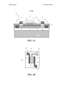
High-voltage GAN high electron mobility transistors
PatentWO2017181121A2
Innovation
- The development of high-voltage HEMTs with a gallium-nitride material structure, including a buffer layer, conduction layer, barrier layer, gate, source, and drain, with a gate-connected field plate extending beyond the gate edges, and a thin gallium-oxide layer formed through oxygen plasma treatment, to enhance reverse-bias voltage withstand and reduce leakage currents.

High electron mobility transistors with improved heat dissipation
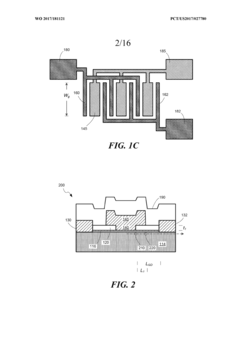
PatentWO2016054545A1
Innovation
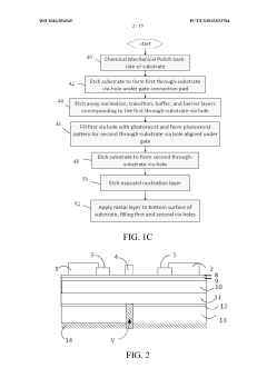
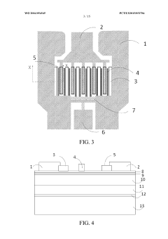
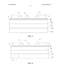
- The method involves etching a via hole through the substrate under the gate or active region of the HEMT to expose and remove the thermally resistive nucleation layer, followed by filling the via hole with metal to enhance heat dissipation, which can be connected to the source, drain, or gate electrodes, and includes forming additional via-holes under the source or gate to act as a field plate and heat sink.
Thermal Management Strategies for GaN HEMT Industrial Applications
Effective thermal management is critical for GaN HEMT devices operating in harsh industrial environments where temperatures can fluctuate dramatically and often exceed normal operating conditions. The superior thermal conductivity of GaN (130 W/m·K) compared to silicon (150 W/m·K) and silicon carbide (490 W/m·K) presents both advantages and challenges for industrial applications.
Advanced substrate materials play a crucial role in thermal management strategies. Silicon carbide (SiC) substrates have emerged as the preferred choice for high-power industrial applications due to their excellent thermal conductivity. Diamond substrates, though still in experimental stages, offer even greater thermal dissipation capabilities with thermal conductivity exceeding 2000 W/m·K, potentially revolutionizing future industrial GaN HEMT implementations.
Package-level thermal solutions have evolved significantly to address industrial requirements. Direct bonded copper (DBC) and active metal brazed (AMB) substrates provide superior thermal pathways while maintaining electrical isolation. Advanced thermal interface materials (TIMs) with enhanced thermal conductivity reduce the thermal resistance between the GaN HEMT die and heat sink, critical for maintaining junction temperatures within safe operating limits in industrial settings.
System-level cooling approaches have diversified beyond traditional air cooling. Liquid cooling systems, including microchannel coolers integrated directly into GaN HEMT packages, have demonstrated the ability to handle power densities exceeding 1000 W/cm². Two-phase cooling technologies utilizing the latent heat of vaporization offer even greater cooling efficiency for the most demanding industrial applications, such as high-power motor drives and industrial power supplies.
Thermal simulation and modeling tools have become essential for optimizing thermal management strategies. Computational fluid dynamics (CFD) coupled with detailed electro-thermal models enable accurate prediction of temperature distributions and hotspots under various industrial operating conditions. These tools allow engineers to evaluate thermal performance before physical prototyping, significantly reducing development cycles for industrial GaN HEMT applications.
Active thermal management techniques incorporating temperature sensors and dynamic power management algorithms provide real-time thermal protection. These systems can adjust operating parameters based on temperature feedback, extending device lifetime in variable industrial environments. Some advanced implementations include predictive thermal management that anticipates temperature rises based on load profiles and adjusts operation preemptively.
Reliability Testing Standards and Certification Requirements
The reliability of GaN HEMT devices in harsh industrial environments necessitates rigorous testing standards and certification requirements to ensure operational stability and longevity. Currently, several established frameworks guide the qualification process for these semiconductor devices, with the Joint Electron Device Engineering Council (JEDEC) standards being particularly prominent. JEDEC's JESD22 series provides comprehensive methodologies for environmental and physical testing, including temperature cycling (JESD22-A104), thermal shock (JESD22-A106), and high-temperature operating life tests (JESD22-A108), which are critical for GaN HEMT reliability assessment.
Automotive Electronics Council's AEC-Q100 qualification represents another significant standard, especially relevant as GaN technology increasingly penetrates industrial automation systems with automotive-grade reliability requirements. This standard defines stress test qualification for integrated circuits, with specific temperature grades that align with industrial operating conditions. For GaN HEMTs intended for harsh environments, Grade 0 (-40°C to +150°C) or Grade 1 (-40°C to +125°C) certifications are typically required.
Military and aerospace applications of GaN HEMTs follow the MIL-STD-750 and MIL-STD-883 standards, which outline test methods for semiconductor devices under extreme conditions. These standards include rigorous radiation hardness testing, which is particularly relevant for GaN HEMTs deployed in environments with potential radiation exposure, such as nuclear facilities or space-adjacent industrial applications.
International Electrotechnical Commission (IEC) standards also play a crucial role, particularly IEC 60747 for discrete semiconductor devices and IEC 61000 series for electromagnetic compatibility. The latter is especially important for GaN HEMTs operating at high frequencies in industrial settings where electromagnetic interference could compromise system integrity.
Specific to power electronics applications, the IEC 62477-1 standard addresses safety requirements for power electronic converter systems, which encompasses many industrial GaN HEMT implementations. Additionally, the emerging JEDEC JEP180 guideline specifically addresses reliability testing for GaN power conversion devices, providing a framework tailored to the unique characteristics of GaN technology.
Certification processes typically involve third-party testing laboratories that verify compliance with these standards. Organizations such as UL (Underwriters Laboratories), TÜV (Technischer Überwachungsverein), and CSA (Canadian Standards Association) provide certification services that are widely recognized in industrial markets. For GaN HEMTs in particular, certification often requires accelerated life testing under combined stressors that simulate harsh industrial conditions, including simultaneous high temperature, humidity, and electrical stress testing.
Unlock deeper insights with Patsnap Eureka Quick Research — get a full tech report to explore trends and direct your research. Try now!
Generate Your Research Report Instantly with AI Agent
Supercharge your innovation with Patsnap Eureka AI Agent Platform!