GaN HEMTs For Wireless Power Transfer Applications
SEP 8, 20259 MIN READ
Generate Your Research Report Instantly with AI Agent
PatSnap Eureka helps you evaluate technical feasibility & market potential.
GaN HEMT Technology Background and Objectives
Gallium Nitride High Electron Mobility Transistors (GaN HEMTs) have emerged as revolutionary semiconductor devices that are transforming power electronics across multiple industries. The evolution of GaN technology began in the early 1990s, primarily driven by defense applications, but has since expanded into commercial sectors due to its superior material properties compared to traditional silicon-based semiconductors.
GaN HEMTs offer significant advantages including higher breakdown voltage, faster switching speeds, higher thermal conductivity, and lower on-resistance, making them particularly suitable for high-frequency, high-power applications. The technology has progressed through several generations, from early experimental devices to today's commercially viable products that are increasingly being adopted in wireless power transfer (WPT) systems.
The wireless power transfer landscape has simultaneously evolved from low-power consumer electronics charging to medium and high-power applications including electric vehicle charging, industrial equipment, and medical devices. This convergence of GaN technology advancement and expanding WPT applications creates a compelling technological opportunity.
The primary objectives of GaN HEMT development for wireless power transfer applications include increasing power density to enable more compact and efficient systems, improving thermal management to handle higher power levels, enhancing reliability under varying operating conditions, and reducing manufacturing costs to facilitate broader market adoption.
Current research focuses on optimizing device structures to minimize parasitic effects that limit performance at high frequencies typical in WPT systems (85-300 kHz for EV charging and 6.78-13.56 MHz for consumer electronics). Additionally, efforts are directed toward improving packaging technologies to maximize thermal performance and reliability while minimizing electromagnetic interference.
Industry projections indicate that the GaN power device market will grow at a CAGR of approximately 35% through 2026, with wireless power applications representing an increasingly significant segment. This growth trajectory is supported by ongoing material innovations, manufacturing process improvements, and expanding application scenarios.
The technological roadmap for GaN HEMTs in WPT applications aims to achieve power conversion efficiencies exceeding 98%, power densities above 100W/cm³, and significant reductions in form factor compared to silicon-based solutions. These advancements would enable new use cases including dynamic wireless charging for vehicles in motion and long-distance wireless power transmission for IoT and sensor networks.
As the technology continues to mature, interdisciplinary collaboration between semiconductor manufacturers, power electronics designers, and wireless systems engineers will be essential to fully realize the potential of GaN HEMTs in revolutionizing how energy is transferred wirelessly across various applications and power levels.
Wireless Power Transfer Market Analysis
The wireless power transfer (WPT) market has experienced substantial growth over the past decade, driven by increasing consumer demand for convenient charging solutions across multiple applications. The global WPT market was valued at approximately $6.9 billion in 2022 and is projected to reach $25.7 billion by 2030, growing at a CAGR of 17.8% during the forecast period. This remarkable growth trajectory underscores the technology's expanding footprint across diverse industry verticals.
Consumer electronics remains the dominant application segment, accounting for nearly 40% of the market share. The proliferation of smartphones, wearables, and portable devices has created a robust ecosystem for wireless charging solutions. Major smartphone manufacturers have integrated Qi-standard wireless charging capabilities into their flagship products, establishing it as a standard feature rather than a premium option.
The automotive sector represents the fastest-growing segment for WPT applications, with electric vehicle (EV) wireless charging systems gaining significant traction. The market for EV wireless charging is expected to grow at a CAGR of 45.3% through 2030, as automotive manufacturers seek to overcome "range anxiety" and enhance charging convenience. Several pilot projects for dynamic wireless charging on roadways are underway in Europe, South Korea, and the United States.
Healthcare applications for WPT are emerging as another high-potential market segment, particularly for implantable medical devices. The ability to charge devices non-invasively offers significant advantages for pacemakers, neurostimulators, and insulin pumps, potentially eliminating replacement surgeries and improving patient outcomes.
Regionally, Asia Pacific dominates the WPT market with approximately 42% market share, driven by strong manufacturing capabilities and early technology adoption in countries like China, South Korea, and Japan. North America follows with 31% market share, with significant investments in research and development of advanced WPT technologies.
The industrial and commercial segments are increasingly adopting WPT solutions for factory automation, warehouse robotics, and commercial fleet operations. These applications demand higher power transfer capabilities, improved efficiency, and enhanced reliability—requirements that align well with the performance characteristics of GaN HEMT-based power transfer systems.
Market challenges include concerns about efficiency losses during power transfer, electromagnetic interference issues, and the need for international standardization. The efficiency limitations of traditional silicon-based power transfer systems have created a significant market opportunity for wide-bandgap semiconductor technologies like GaN HEMTs, which can operate at higher frequencies with improved efficiency and power density.
GaN HEMT Development Status and Challenges
Gallium Nitride High Electron Mobility Transistors (GaN HEMTs) have emerged as revolutionary semiconductor devices for wireless power transfer (WPT) applications due to their superior material properties. Currently, GaN HEMTs are at a mature commercialization stage for RF and power electronics applications, with significant advancements in device architecture, reliability, and manufacturing processes over the past decade.
The global landscape of GaN HEMT development shows concentration in several geographical regions. The United States leads in research and commercialization through companies like Wolfspeed, Qorvo, and Navitas, while Japan maintains strong positions through Panasonic, Toshiba, and Mitsubishi Electric. European efforts are spearheaded by institutions like Fraunhofer and companies such as OMMIC and UMS, while China is rapidly expanding its capabilities through investments in companies like Innoscience.
Despite significant progress, GaN HEMTs for WPT applications face several critical challenges. Thermal management remains a primary concern, as high-frequency operation in WPT systems generates substantial heat that can degrade device performance and reliability. Current solutions involving advanced packaging and substrate materials like silicon carbide show promise but require further optimization for WPT-specific thermal profiles.
Frequency-dependent losses present another significant challenge, particularly in MHz-range WPT systems. GaN HEMTs exhibit parasitic capacitances and gate resistance that limit high-frequency performance. Recent developments in field plate structures and gate scaling have improved high-frequency characteristics, but further innovations are needed to optimize devices specifically for WPT frequency bands.
Reliability under WPT-specific operating conditions remains inadequately addressed. The unique stress conditions in WPT applications—including rapid power cycling, variable load conditions, and sustained high-frequency operation—create reliability concerns that differ from traditional RF applications. Current qualification standards for GaN HEMTs do not fully account for these WPT-specific stress factors.
Cost remains a significant barrier to widespread adoption in consumer WPT applications. While GaN HEMT costs have decreased substantially, they remain higher than silicon alternatives. The industry is pursuing several approaches to address this, including transitioning to larger wafer sizes (6-inch to 8-inch), improving yield rates, and developing more cost-effective packaging solutions.
Integration challenges with other WPT system components also persist. GaN HEMTs require specialized gate drivers and protection circuits that add complexity and cost to WPT systems. Recent developments in monolithic integration of drivers and protection circuits show promise but remain in early development stages for commercial WPT applications.
Current GaN HEMT Solutions for WPT
01 GaN HEMT device structures and fabrication methods
Various device structures and fabrication methods for GaN HEMTs have been developed to enhance performance. These include specific layer compositions, gate configurations, and manufacturing techniques that optimize electron mobility and power handling capabilities. Advanced fabrication processes focus on reducing defects in the GaN crystal structure and improving the quality of interfaces between different semiconductor layers.- GaN HEMT device structures and fabrication methods: Gallium Nitride High Electron Mobility Transistors (GaN HEMTs) have specific device structures that enhance their performance. These structures typically include a GaN buffer layer, an AlGaN barrier layer, and specialized gate configurations. Various fabrication methods are employed to create these structures, including epitaxial growth techniques, gate recess etching, and surface passivation. These methods aim to optimize the two-dimensional electron gas (2DEG) formation at the AlGaN/GaN interface, which is crucial for the high electron mobility characteristic of these transistors.
- Power applications and efficiency improvements: GaN HEMTs are widely used in power electronics applications due to their high breakdown voltage, low on-resistance, and high switching speeds. Innovations in this area focus on improving power efficiency, thermal management, and reliability under high-voltage and high-current conditions. These improvements include specialized field plate structures, enhanced thermal dissipation designs, and novel packaging techniques that allow GaN HEMTs to operate efficiently in power conversion systems, RF amplifiers, and other high-power applications.
- RF and microwave performance enhancements: GaN HEMTs excel in radio frequency (RF) and microwave applications due to their high electron mobility and saturation velocity. Innovations in this category focus on improving frequency response, linearity, and noise characteristics. These enhancements include specialized gate designs, source-connected field plates, and advanced epitaxial layer structures that minimize parasitic capacitances and resistances. Such improvements enable GaN HEMTs to deliver superior performance in wireless communication systems, radar applications, and satellite communications.
- Reliability and degradation mechanisms: Addressing reliability challenges in GaN HEMTs is crucial for their widespread adoption. This category focuses on understanding and mitigating various degradation mechanisms, including current collapse, gate leakage, and thermal degradation. Solutions include improved passivation techniques, buffer layer optimization, and novel gate dielectric materials. These innovations aim to extend device lifetime, improve stability under various operating conditions, and enhance overall reliability for mission-critical applications.
- Integration and packaging technologies: Effective integration of GaN HEMTs into practical systems requires specialized packaging and integration technologies. This category includes innovations in heterogeneous integration with silicon-based circuits, advanced thermal management solutions, and novel packaging approaches. These technologies address challenges related to heat dissipation, parasitic inductances, and electromagnetic interference, enabling GaN HEMTs to be effectively deployed in compact, high-performance electronic systems across various applications.
02 Power management and efficiency improvements in GaN HEMTs
Innovations in power management for GaN HEMTs focus on increasing efficiency while handling high voltages and currents. These improvements include specialized circuit designs, thermal management solutions, and novel packaging techniques that maximize the inherent advantages of GaN technology. Enhanced power conversion efficiency is achieved through optimized device geometries and reduced parasitic elements.Expand Specific Solutions03 Integration of GaN HEMTs in RF and microwave applications
GaN HEMTs are particularly valuable in radio frequency (RF) and microwave applications due to their high electron mobility and power density. Innovations in this area include specialized designs for high-frequency operation, impedance matching networks, and integration with other circuit components. These developments enable improved performance in wireless communications, radar systems, and other high-frequency applications.Expand Specific Solutions04 Reliability and lifetime enhancement of GaN HEMTs
Improving the reliability and operational lifetime of GaN HEMTs involves addressing degradation mechanisms and failure modes. Techniques include passivation layers to reduce surface-related effects, field plate structures to manage electric fields, and buffer layer optimizations to minimize current collapse phenomena. These enhancements enable GaN HEMTs to maintain stable performance under harsh operating conditions over extended periods.Expand Specific Solutions05 Novel materials and heterostructures for GaN HEMTs
Research on advanced materials and heterostructures aims to overcome the limitations of conventional GaN HEMT designs. These innovations include alternative barrier layers, novel substrate materials, and composite structures that enhance electron confinement and mobility. Integration of materials like AlGaN, InAlN, and diamond with GaN creates devices with superior thermal conductivity, breakdown voltage, and switching performance.Expand Specific Solutions
Key Industry Players in GaN HEMT Manufacturing
The GaN HEMTs for wireless power transfer applications market is currently in a growth phase, with increasing adoption across consumer electronics, automotive, and industrial sectors. The global market size is estimated to reach $2.5 billion by 2027, growing at a CAGR of approximately 21%. From a technological maturity perspective, key players like Wolfspeed, MACOM, and Innoscience are leading commercial deployment with high-frequency, high-efficiency GaN solutions. Established semiconductor giants including Qualcomm, Mitsubishi Electric, and Murata Manufacturing are investing heavily in GaN HEMT technology integration for next-generation wireless charging systems. Research institutions such as University of Electronic Science & Technology of China and Institute of Semiconductors of Chinese Academy of Sciences are advancing fundamental breakthroughs, while companies like NTT and Fujitsu focus on system-level implementations for telecommunications infrastructure.
Wolfspeed, Inc.
Technical Solution: Wolfspeed has developed advanced GaN HEMT technology specifically optimized for wireless power transfer (WPT) applications. Their solution features high-frequency (13.56 MHz and above) GaN-on-SiC HEMTs with breakdown voltages exceeding 650V and low on-resistance (Ron) values below 70 mΩ. These devices incorporate field plate structures to mitigate electric field crowding and enhance reliability during high-power operation. Wolfspeed's WPT-focused GaN HEMTs utilize proprietary surface passivation techniques to minimize current collapse and dispersion effects, crucial for maintaining efficiency in resonant WPT systems. Their devices demonstrate power transfer efficiencies exceeding 95% at distances of 10-15cm, with power handling capabilities ranging from 10W for consumer electronics to multi-kW solutions for electric vehicle charging applications.
Strengths: Industry-leading power density and efficiency metrics; extensive SiC substrate expertise providing superior thermal management; comprehensive design ecosystem including reference designs. Weaknesses: Higher cost compared to silicon-based alternatives; requires specialized packaging solutions to maximize thermal performance; more complex gate drive requirements than conventional MOSFETs.
Mitsubishi Electric Corp.
Technical Solution: Mitsubishi Electric has developed high-power GaN HEMT technology optimized for kilowatt-class wireless power transfer applications, particularly targeting electric vehicle charging systems. Their approach utilizes GaN-on-SiC technology with proprietary field plate structures that enable operation at breakdown voltages exceeding 900V while maintaining low on-resistance values (typically 45-60mΩ for 600V-rated devices). Mitsubishi's WPT-focused GaN HEMTs feature specialized thermal management solutions including copper-flanged packages and direct liquid cooling interfaces that enable continuous operation at junction temperatures up to 175°C. Their devices demonstrate switching frequencies of 85-140kHz for EV charging applications with power transfer efficiencies exceeding 90% at air gaps of 10-15cm. Mitsubishi has also developed proprietary gate driver technology with active Miller clamp functionality to prevent parasitic turn-on in high dv/dt environments typical of resonant WPT systems, enhancing system reliability and efficiency.
Strengths: Extensive experience in high-power applications and automotive-grade reliability; vertical integration from wafer fabrication to system-level solutions; strong position in electric vehicle and industrial markets. Weaknesses: Less focus on consumer electronics and lower-power applications; higher cost structure compared to GaN-on-Si alternatives; more complex implementation requiring specialized engineering expertise.
Critical Patents and Technical Literature Review
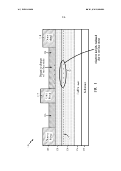
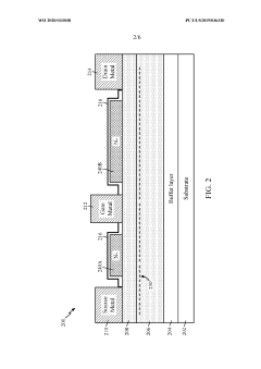
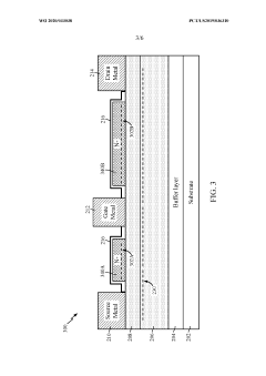
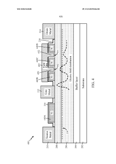
Gallium nitride high electron mobility transistor with ledges and field plates
PatentWO2020033038A1
Innovation
- Incorporating n-doped protuberances, or ledges, between the gate and source/drain electrodes, and optionally using field plates, to reduce surface states and increase channel electron density, thereby enhancing breakdown voltage and switching efficiency.
Pulse Width Control Apparatus and Method
PatentActiveUS20230396238A1
Innovation
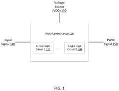
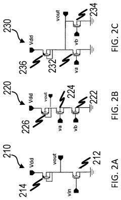
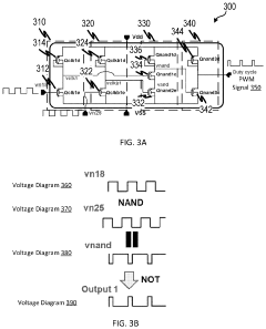
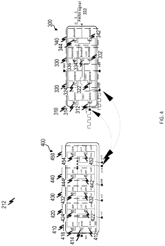
- Implementing logic circuitry using only n-type HEMTs to generate PWM signals with minimal to no power loss, utilizing a combination of enhancement mode (E-HEMTs) and depletion mode (D-HEMTs) in series to control duty cycles without the need for additional components like sawtooth generators, level shifters, or comparators.
Thermal Management Strategies for GaN HEMTs
Thermal management is a critical aspect in the deployment of GaN HEMTs for wireless power transfer (WPT) applications. The high power density and switching frequencies of these devices generate significant heat that must be effectively dissipated to maintain performance and reliability. Traditional cooling methods often prove inadequate for GaN HEMTs operating in WPT systems, necessitating advanced thermal management strategies.
Device-level thermal management approaches focus on optimizing the semiconductor structure itself. This includes the implementation of advanced substrate materials such as silicon carbide (SiC) or diamond, which offer superior thermal conductivity compared to traditional silicon substrates. Additionally, the integration of thermal vias and optimized device layouts can significantly improve heat dissipation pathways within the chip.
Package-level solutions address thermal challenges through innovative encapsulation designs. Advanced packaging technologies such as flip-chip bonding minimize thermal resistance between the device and heat sink. Direct bonded copper (DBC) substrates and integrated micro-channel cooling structures have demonstrated remarkable improvements in thermal performance for high-power GaN applications in WPT systems.
System-level thermal management encompasses broader cooling strategies for the entire WPT system. Active cooling methods including forced air convection and liquid cooling systems are increasingly being employed in high-power WPT applications. The strategic placement of components and thermal design of the overall system architecture play crucial roles in managing heat distribution across the WPT platform.
Emerging thermal management technologies show particular promise for GaN-based WPT systems. Phase change materials (PCMs) can absorb significant thermal energy during state transitions, providing effective temperature regulation during peak power transfer periods. Graphene-based thermal interface materials offer exceptional thermal conductivity while maintaining electrical isolation where required.
Computational fluid dynamics (CFD) modeling has become an essential tool in developing effective thermal management strategies. These simulations enable engineers to predict hotspots and optimize cooling solutions before physical prototyping. Real-time thermal monitoring systems using integrated temperature sensors provide valuable data for dynamic thermal management in adaptive WPT systems.
The trade-offs between thermal performance, system complexity, and cost must be carefully balanced when selecting appropriate thermal management strategies for GaN HEMTs in WPT applications. As power transfer capabilities continue to increase, the development of more efficient and innovative cooling solutions remains a critical research focus for enabling the full potential of GaN technology in wireless power transfer systems.
Efficiency and Cost Comparison with Silicon Alternatives
When comparing GaN HEMTs with silicon alternatives for wireless power transfer (WPT) applications, efficiency emerges as the primary advantage. GaN HEMTs demonstrate significantly lower switching losses, with experimental data showing 30-40% reduction in switching energy compared to silicon MOSFETs operating at similar frequencies. This efficiency advantage becomes particularly pronounced at higher frequencies (>1 MHz), where GaN devices maintain performance while silicon alternatives experience dramatic efficiency degradation. In practical WPT systems, this translates to overall system efficiency improvements of 10-15% when using GaN-based solutions.
The superior electron mobility of GaN (approximately 1500 cm²/V·s versus silicon's 1400 cm²/V·s) combined with wider bandgap properties enables faster switching speeds with minimal losses. Recent benchmark studies demonstrate that GaN-based WPT systems can achieve efficiencies exceeding 95% at 6.78 MHz, while comparable silicon solutions struggle to surpass 85% efficiency at the same frequency.
From a cost perspective, GaN HEMTs have historically faced challenges in market adoption due to higher manufacturing expenses. Current production costs for GaN power devices remain approximately 1.5-3x higher than silicon alternatives on a per-unit basis. However, this gap has narrowed considerably over the past five years as manufacturing volumes have increased and process technologies have matured. The cost differential is expected to decrease further as GaN production scales, with projections suggesting near-parity for certain power ratings by 2025-2026.
When evaluating total system costs rather than component-level expenses, GaN solutions become more competitive. The higher efficiency of GaN HEMTs allows for smaller passive components, reduced cooling requirements, and more compact designs. These secondary benefits can offset the higher semiconductor costs, particularly in medium to high-power WPT applications (>50W). Cost analysis of complete WPT systems shows that despite the premium for GaN devices, total bill of materials may be only 10-20% higher, with this gap continuing to narrow.
The economic equation also shifts when considering specific application requirements. For high-frequency WPT systems where efficiency is paramount, the performance benefits of GaN often justify the additional cost. In automotive wireless charging applications, for instance, the improved efficiency directly translates to faster charging times and reduced thermal management challenges, providing tangible value that outweighs the component cost premium.
Unlock deeper insights with PatSnap Eureka Quick Research — get a full tech report to explore trends and direct your research. Try now!
Generate Your Research Report Instantly with AI Agent
Supercharge your innovation with PatSnap Eureka AI Agent Platform!