

HBM4 Interposer Stitching: Yield, Alignment And Electrical Continuity
SEP 12, 20259 MIN READ
Generate Your Research Report Instantly with AI Agent
PatSnap Eureka helps you evaluate technical feasibility & market potential.
HBM4 Interposer Stitching Background and Objectives
High Bandwidth Memory (HBM) technology has evolved significantly since its introduction, with HBM4 representing the latest advancement in this critical memory architecture. The development trajectory from HBM1 through HBM4 demonstrates a consistent focus on increasing bandwidth, reducing power consumption, and enhancing overall system performance for data-intensive applications. HBM4 builds upon previous generations by further pushing the boundaries of memory density, speed, and integration capabilities.
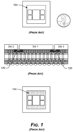
Interposer technology has been fundamental to HBM implementation, serving as the critical substrate that connects memory stacks to processing units. Traditional interposer designs have faced size limitations due to manufacturing constraints, particularly in reticle field size restrictions. This limitation has become increasingly problematic as computing systems demand ever-larger memory arrays and more complex integration schemes.
Interposer stitching emerged as a revolutionary approach to overcome these size limitations by joining multiple smaller interposer segments to create larger effective interposer areas. This technique has evolved from experimental implementations to becoming a necessary enabler for advanced HBM4 deployments, particularly in high-performance computing, AI accelerators, and data center applications.
The primary technical objectives for HBM4 interposer stitching focus on three critical aspects: yield improvement, precise alignment, and electrical continuity. Yield challenges stem from the inherent complexity of manufacturing and joining multiple silicon segments with minimal defects. As interposer dimensions increase through stitching, maintaining economically viable yields becomes exponentially more challenging.
Alignment precision represents another fundamental objective, as misalignment between interposer segments can lead to signal integrity issues, increased parasitic effects, and potential connection failures. The industry aims to achieve sub-micron alignment precision consistently across large stitched interposer areas to support the fine-pitch interconnects required by HBM4.
Electrical continuity across stitched interfaces presents unique challenges related to resistance matching, signal integrity preservation, and thermal management. The technical goal is to create seamless electrical pathways across stitched boundaries that perform identically to monolithic interposer designs, ensuring that data transfer rates and signal quality meet HBM4 specifications.
The evolution of interposer stitching technology is closely tied to broader semiconductor manufacturing trends, including advanced packaging innovations, heterogeneous integration capabilities, and chiplet-based design approaches. As computing architectures increasingly rely on memory-intensive workloads, particularly for AI and machine learning applications, the importance of solving these technical challenges has elevated interposer stitching from a specialized technique to a mainstream enabling technology.
Market Demand Analysis for Advanced Packaging Solutions
The advanced packaging market is experiencing unprecedented growth driven by the increasing demand for high-performance computing, artificial intelligence, and data-intensive applications. HBM4 (High Bandwidth Memory) technology with interposer stitching represents a critical advancement in this space, addressing the need for greater memory bandwidth and capacity while maintaining power efficiency.
Market research indicates that the global advanced packaging market is projected to grow at a CAGR of 8.2% from 2023 to 2028, with the memory segment being one of the fastest-growing categories. The demand for HBM solutions specifically is expected to surge as data centers, AI accelerators, and high-performance computing platforms require ever-increasing memory performance.
Interposer-based packaging solutions, particularly those employing stitching techniques for larger effective die areas, are gaining significant traction in the semiconductor industry. This growth is primarily driven by the limitations of traditional packaging approaches in meeting the interconnect density and bandwidth requirements of next-generation computing systems.
The HBM4 standard, with its promise of higher bandwidth, increased capacity, and improved power efficiency compared to HBM3, is positioned to capture a substantial portion of the high-end memory market. Industry analysts predict that by 2026, over 40% of AI accelerator cards will incorporate some form of HBM technology, with HBM4 expected to become the dominant standard by 2027.
Key market segments driving demand for advanced interposer solutions include cloud service providers, who are investing heavily in AI infrastructure; telecommunications companies deploying edge computing solutions; and scientific research institutions requiring extreme computational capabilities. These segments collectively represent a market opportunity exceeding $15 billion annually for advanced packaging technologies.
Customer requirements are increasingly focused on reliability metrics, with yield and electrical continuity being primary concerns. Survey data from major semiconductor customers indicates that over 85% consider yield improvements in interposer stitching to be "very important" or "critical" for adoption of next-generation HBM solutions.
Regional analysis shows that while North America leads in terms of technology development, Asia-Pacific represents the largest market for implementation, with Taiwan, South Korea, and China being particularly significant. European demand is growing steadily, primarily in automotive and industrial applications requiring high-reliability memory solutions.
The economic value proposition of improved interposer stitching techniques is compelling. Cost modeling suggests that a 5% improvement in yield can translate to approximately $50-70 million in annual savings for a high-volume manufacturer, highlighting the significant market incentive for technological advancement in this area.
Technical Challenges in Interposer Stitching Implementation
Interposer stitching technology for HBM4 implementation faces several significant technical challenges that must be addressed to ensure successful integration. The primary challenge lies in achieving high yield rates during the manufacturing process. Traditional interposer fabrication typically involves creating a single large silicon interposer, which becomes increasingly difficult and costly as size requirements grow for advanced HBM4 applications. The yield rate decreases exponentially with increased interposer size due to the higher probability of defects occurring across larger silicon areas.
Alignment precision represents another critical challenge in interposer stitching. When multiple smaller interposer segments are stitched together, micron-level alignment accuracy is required to ensure proper functionality. Current lithography and placement tools struggle to maintain consistent sub-micron alignment across multiple interposer segments, particularly when thermal expansion and contraction factors come into play during various manufacturing stages. Even minor misalignments can lead to catastrophic connection failures between HBM4 memory stacks and the underlying compute die.
Electrical continuity across stitched interfaces presents perhaps the most complex technical hurdle. Creating seamless electrical pathways between separate interposer segments requires innovative interconnect solutions that can bridge the physical gaps while maintaining signal integrity. Engineers must develop specialized trace routing techniques that can traverse the stitching boundaries without introducing excessive resistance, capacitance, or inductance that would degrade high-speed signal performance critical for HBM4 operation.
Thermal management complications arise from the discontinuities at stitching interfaces. These junctions can create thermal bottlenecks that impede efficient heat dissipation from both memory and compute elements. The resulting hotspots may lead to performance throttling or reliability issues, particularly under heavy computational loads when HBM4 memory bandwidth is fully utilized.
Manufacturing process compatibility presents additional challenges, as interposer stitching requires precise coordination between multiple fabrication steps. The process must accommodate different materials with varying coefficients of thermal expansion while maintaining dimensional stability throughout thermal cycles. Furthermore, inspection and testing methodologies must evolve to effectively evaluate the quality of stitched interfaces, which traditional testing approaches may not adequately assess.
Cost considerations remain a significant barrier to widespread adoption of interposer stitching technology. While stitching potentially improves overall yield by using smaller interposer segments, the additional processing steps and specialized equipment required for precise alignment and bonding introduce new costs that must be carefully balanced against the yield benefits to ensure economic viability for high-volume HBM4 applications.
Current Yield Enhancement Methodologies for Stitched Interposers
01 Interposer stitching techniques for HBM4 yield improvement
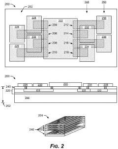
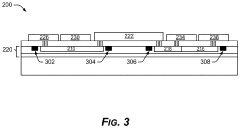
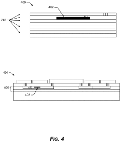
Various stitching techniques are employed in HBM4 interposer manufacturing to improve yield. These techniques involve connecting multiple smaller interposer segments to form a larger functional unit, which helps overcome size limitations in manufacturing equipment and reduces defect rates. Advanced lithography and etching processes ensure precise alignment between stitched segments, while specialized testing methods verify the integrity of connections across stitched boundaries.- Interposer stitching techniques for HBM4 integration: Advanced interposer stitching techniques are essential for high-bandwidth memory (HBM4) integration. These techniques involve connecting multiple silicon dies on an interposer substrate to create a high-performance package. The stitching process requires precise alignment and bonding methods to ensure proper electrical connections between the memory dies and logic chips. Innovations in this area focus on reducing the gap between stitched components and ensuring uniform connections across the interposer surface.
- Alignment methods for high-yield interposer manufacturing: Precise alignment is critical for successful interposer stitching in HBM4 applications. Various alignment methods have been developed to ensure accurate positioning of components during the manufacturing process. These include optical alignment systems, mechanical alignment features, and feedback-controlled positioning mechanisms. Advanced alignment techniques can compensate for thermal expansion differences and substrate warpage, significantly improving manufacturing yield and reliability of the final assembled package.
- Electrical continuity testing and verification in interposer assemblies: Ensuring electrical continuity across stitched interposers is crucial for HBM4 performance. Testing methodologies have been developed to verify the integrity of electrical connections between dies and through the interposer substrate. These include in-line testing during manufacturing, post-assembly verification, and specialized probe techniques for high-density interconnects. Advanced testing approaches can detect micro-cracks, partial connections, and other defects that might impact signal integrity or power delivery in the assembled package.
- Thermal management solutions for stitched interposer packages: Thermal management is a significant challenge in HBM4 interposer assemblies due to high power density and the presence of multiple heat-generating components. Solutions include integrated cooling channels, advanced thermal interface materials, and optimized heat spreading designs. Effective thermal management directly impacts yield and reliability by preventing thermal-induced stress and maintaining optimal operating temperatures across the interposer assembly, which is particularly important for maintaining alignment integrity during operation.
- Materials and manufacturing processes for high-reliability interposer connections: Advanced materials and manufacturing processes have been developed specifically for HBM4 interposer applications to improve yield and reliability. These include specialized underfill materials, low-temperature bonding techniques, and novel interconnect structures. Manufacturing innovations focus on reducing stress at connection points, improving adhesion between different materials, and enhancing the overall mechanical stability of the assembly. These advancements help maintain electrical continuity throughout thermal cycling and mechanical stress events.
02 Alignment methods for interposer manufacturing
Precise alignment is critical in HBM4 interposer manufacturing to ensure proper electrical connections between stitched segments. Optical alignment systems using fiducial markers provide sub-micron precision for positioning interposer segments. Advanced metrology tools monitor alignment during the manufacturing process, allowing for real-time adjustments. Some methods incorporate self-aligning features in the interposer design to compensate for minor misalignments during assembly.Expand Specific Solutions03 Electrical continuity verification in stitched interposers
Ensuring electrical continuity across stitched boundaries in HBM4 interposers requires specialized testing methods. Automated test equipment verifies signal integrity across stitched interfaces using high-frequency probing techniques. Non-destructive testing methods such as X-ray inspection and time-domain reflectometry identify potential discontinuities at stitch points. Redundant routing paths are often implemented to maintain electrical performance even if some connections fail, improving overall yield.Expand Specific Solutions04 Materials and structures for reliable interposer connections
Advanced materials and structural designs enhance the reliability of HBM4 interposer connections. Low-CTE (coefficient of thermal expansion) materials minimize stress at stitched interfaces during thermal cycling. Multi-layer redistribution structures with specialized vias maintain signal integrity across stitched boundaries. Novel interconnect designs using copper pillars or through-silicon vias (TSVs) improve electrical performance while accommodating manufacturing tolerances at stitch points.Expand Specific Solutions05 Testing and quality control for interposer stitching
Comprehensive testing and quality control processes are essential for achieving high yields in HBM4 interposer stitching. In-line optical inspection systems detect misalignments and defects during the manufacturing process. Electrical parametric testing verifies signal integrity across stitched boundaries under various operating conditions. Known-good-die testing methodologies are adapted for interposer segments to identify defects before final assembly, significantly improving overall yield and reducing costs.Expand Specific Solutions
Key Industry Players in HBM4 Interposer Manufacturing
The HBM4 Interposer Stitching technology market is currently in an early growth phase, characterized by increasing demand for advanced packaging solutions in high-performance computing applications. The market size is expanding rapidly, driven by AI acceleration and data center requirements, with projections suggesting a compound annual growth rate exceeding 25% through 2027. From a technical maturity perspective, key players demonstrate varying levels of advancement: Intel, Samsung, and GLOBALFOUNDRIES lead with established interposer manufacturing capabilities, while Xilinx (now part of AMD) has pioneered multi-die integration techniques. IBM and Google are focusing on electrical continuity innovations, with emerging contributions from Chinese entities like BOE Technology and Shanghai Xinwei Semiconductor, though they currently lag in yield optimization and precision alignment technologies critical for HBM4 implementation.
Xilinx, Inc.
Technical Solution: Xilinx has developed a specialized interposer stitching technology for HBM4 integration that focuses on maximizing yield through a modular approach. Their solution employs a "known good die" methodology where individual interposer segments are fully tested before final assembly, significantly reducing waste of expensive silicon. For alignment precision, Xilinx utilizes a proprietary optical feedback system that continuously monitors and adjusts positioning during the bonding process, achieving alignment accuracy of approximately 0.3μm. Their electrical continuity solution features redundant microbump arrays at stitching interfaces with intelligent signal routing that can bypass defective connections. Additionally, Xilinx has implemented specialized test structures embedded within the interposer design that allow for comprehensive electrical verification before and after assembly, enabling early detection of potential failures.
Strengths: Modular "known good die" approach significantly improves yield rates and reduces costs. Their embedded test structures enable comprehensive verification at multiple stages. Weaknesses: The additional testing steps increase manufacturing time, and their approach requires more complex signal routing which can impact performance in some applications.
International Business Machines Corp.
Technical Solution: IBM has developed an innovative approach to HBM4 interposer stitching that leverages their expertise in advanced packaging technologies. Their solution utilizes a silicon bridge architecture with specialized "stitching corridors" that contain redundant interconnect pathways to maintain electrical continuity even when defects occur. IBM's manufacturing process incorporates precision alignment techniques using infrared alignment systems that can achieve positioning accuracy of approximately 0.4μm across large interposer areas. For yield improvement, they've implemented a multi-stage testing methodology that identifies defects at each assembly step, allowing for early rejection of faulty components. IBM's approach also includes specialized metallization processes at stitching interfaces that create self-forming interconnects, which can accommodate minor misalignments while maintaining electrical performance. Their technology incorporates thermal compensation mechanisms that adjust for expansion differences between materials during the high-temperature bonding processes.
Strengths: Advanced infrared alignment systems provide excellent positioning accuracy across large interposers. Their redundant "stitching corridors" significantly improve electrical continuity and fault tolerance. Weaknesses: The specialized metallization processes increase manufacturing complexity and cost, and their approach requires precise thermal management during assembly.
Critical Patents and Research on Alignment Precision
Embedded organic interposer for high bandwidth
PatentPendingUS20210327851A1
Innovation
- Embedded organic interposers with thicker conductors and additional routing layers are embedded within the package core, providing more dielectric space and reducing the resistive-capacitive (RC) load to achieve higher bandwidth transmission, up to 20-60 GHz over longer spans.
Integrated circuit package for high bandwidth memory
PatentActiveUS12315860B2
Innovation
- The implementation of wider channels connecting the HBM stack to the logic die allows for the use of printed traces, such as organic traces, instead of silicon interposer channels, reducing material costs and simplifying production.
Thermal Management Considerations for HBM4 Implementations
Thermal management represents a critical challenge in HBM4 interposer stitching implementations due to the increased power density and thermal constraints inherent in advanced packaging technologies. The thermal considerations become particularly significant when multiple HBM4 stacks are integrated alongside high-performance processors on a single interposer platform.
The stitched interposer design creates unique thermal pathways that must be carefully managed to prevent localized hotspots and thermal gradients. These thermal issues can directly impact the alignment precision during the stitching process, as differential thermal expansion between materials can cause misalignment at critical interfaces. Furthermore, excessive temperatures can compromise the electrical continuity across stitched boundaries.
HBM4's increased bandwidth capabilities (projected to exceed 8TB/s) generate substantially more heat than previous generations, requiring innovative cooling solutions specifically designed for stitched interposer configurations. The thermal interface materials (TIMs) used between the HBM stacks and heat spreaders must maintain performance across the stitched boundaries without introducing additional stress that could affect yield.
Advanced computational fluid dynamics (CFD) modeling has become essential for predicting thermal behavior across stitched interposers. These simulations must account for the discontinuities at stitching boundaries and their impact on heat dissipation pathways. Recent research indicates that thermal gradients exceeding 15°C across stitching interfaces can significantly reduce yield rates by up to 30%.
Liquid cooling solutions are increasingly being explored for HBM4 implementations, with direct-to-chip liquid cooling showing promise for managing the extreme thermal loads. These systems must be designed to accommodate the unique geometry of stitched interposers while ensuring uniform cooling across the entire assembly.
The reliability of electrical connections across stitched boundaries is heavily dependent on thermal cycling performance. Studies show that thermal cycling between -40°C and 125°C can induce stress at stitching interfaces, potentially compromising electrical continuity. Novel underfill materials with enhanced thermal properties are being developed to mitigate these effects.
Emerging technologies such as embedded microfluidic cooling channels within the interposer substrate show promise for next-generation thermal management. These approaches could potentially address both the yield and alignment challenges by providing more uniform temperature distribution across the stitched interposer assembly, thereby reducing thermally-induced stress and warpage.
Cost-Performance Trade-offs in Interposer Stitching Solutions
Interposer stitching for HBM4 integration presents significant cost-performance trade-offs that system architects and manufacturers must carefully navigate. The primary economic consideration stems from the manufacturing yield challenges inherent in large silicon interposers. As interposer size increases to accommodate multiple HBM4 stacks, yield decreases exponentially, driving up costs. Stitching technology offers a compelling alternative by enabling smaller interposer segments to be combined, substantially improving overall yield rates and reducing material waste.
However, this cost advantage comes with performance implications. The stitching interfaces introduce additional electrical discontinuities that can impact signal integrity, particularly for high-speed connections crossing stitch boundaries. These discontinuities may necessitate more conservative design rules, potentially limiting bandwidth or requiring additional signal conditioning circuitry that partially offsets the cost savings.
Manufacturing complexity represents another dimension of this trade-off. While stitched interposers reduce material costs, they require sophisticated alignment equipment and processes to ensure precise positioning of interposer segments. This precision equipment and the associated calibration and maintenance procedures add to the capital expenditure and operational costs, creating a complex cost equation that varies with production volume.
Thermal management considerations further complicate the cost-performance balance. Stitched interfaces may create thermal resistance boundaries that affect heat dissipation from HBM4 modules. Enhanced thermal solutions to address these challenges can add cost and design complexity, particularly in high-performance computing applications where thermal constraints are already significant.
Time-to-market factors also influence the cost-performance equation. While established interposer technologies offer predictable development cycles, stitching approaches may require additional validation and reliability testing, potentially extending development timelines. This extended development must be weighed against the long-term cost benefits of improved yield and material utilization.
Ultimately, the optimal solution depends on specific application requirements and production volumes. High-volume applications with extreme performance demands may justify the premium for monolithic interposers, while cost-sensitive applications with moderate performance requirements may benefit more from stitched solutions. As stitching technology matures, this cost-performance gap is expected to narrow, potentially making stitched interposers the preferred solution across a broader range of applications.
Unlock deeper insights with PatSnap Eureka Quick Research — get a full tech report to explore trends and direct your research. Try now!
Generate Your Research Report Instantly with AI Agent
Supercharge your innovation with PatSnap Eureka AI Agent Platform!