HBM4 TSV Pitch: Density Targets And SI/PI Trade-Offs
SEP 12, 20259 MIN READ
Generate Your Research Report Instantly with AI Agent
Patsnap Eureka helps you evaluate technical feasibility & market potential.
HBM4 TSV Technology Evolution and Objectives
Through Silicon Via (TSV) technology has been a cornerstone of High Bandwidth Memory (HBM) development since its inception, enabling vertical integration of memory dies in a stacked configuration. The evolution of TSV technology in HBM has been characterized by continuous miniaturization and increased density to meet the growing demands for higher bandwidth, capacity, and power efficiency in high-performance computing applications.
The first generation of HBM utilized TSVs with a pitch of approximately 50μm, which was considered advanced at that time. As HBM2 emerged, TSV pitch reduced to around 40μm, enabling higher interconnect density. HBM2E further refined this technology, while maintaining similar TSV dimensions but improving signal integrity characteristics. The current HBM3 standard has pushed TSV pitch down to approximately 30μm, representing significant progress in manufacturing capabilities.
For the upcoming HBM4 standard, industry targets are focusing on TSV pitches in the 20-25μm range, which presents substantial technical challenges but offers tremendous benefits in terms of interconnect density and overall memory performance. This evolution reflects a consistent trend of approximately 20-30% reduction in TSV pitch with each new HBM generation.
The primary objectives driving HBM4 TSV development include achieving higher bandwidth density, supporting increased memory capacity, and maintaining or improving power efficiency metrics. Specifically, HBM4 aims to deliver bandwidth exceeding 8 GT/s per pin, representing a significant improvement over HBM3's capabilities. This requires not only tighter TSV pitch but also enhanced signal and power integrity characteristics.
Another critical objective is enabling higher capacity memory stacks without compromising reliability or thermal performance. The industry is targeting HBM4 configurations with up to 24GB per stack, necessitating either more memory dies in the stack or higher density memory dies, both of which place additional demands on TSV technology.
Power efficiency remains a paramount concern, with HBM4 targeting improved pJ/bit metrics compared to previous generations. This requires careful optimization of TSV electrical characteristics, including capacitance, resistance, and inductance parameters, which become increasingly challenging as dimensions shrink.
Manufacturing yield is also a key consideration in TSV evolution. As pitch decreases, the complexity of fabrication increases substantially, potentially impacting production costs. Therefore, a balance must be struck between pushing the technological boundaries and maintaining economically viable manufacturing processes.
The trajectory of TSV technology for HBM4 represents a critical inflection point where fundamental physical limitations are beginning to constrain further scaling, necessitating innovative approaches to continue the performance scaling trend that has characterized HBM evolution to date.
Market Demand Analysis for High-Density Memory Solutions
The demand for high-density memory solutions has been accelerating dramatically across multiple sectors, driven primarily by data-intensive applications such as artificial intelligence, machine learning, high-performance computing, and advanced graphics processing. The HBM (High Bandwidth Memory) technology, particularly the upcoming HBM4 standard, represents a critical response to these escalating requirements.
Data center operators and cloud service providers are experiencing unprecedented memory bandwidth demands, with AI training models requiring exponentially increasing memory capacity and bandwidth. According to industry analyses, AI model complexity has been doubling approximately every 3.5 months, creating memory requirements that grow at rates far exceeding traditional computing applications.
The automotive and edge computing sectors are emerging as significant new markets for high-density memory solutions. Advanced driver-assistance systems (ADAS) and autonomous driving technologies require substantial memory bandwidth for real-time processing of sensor data. Similarly, edge AI applications demand memory solutions that balance performance with power efficiency.
Market research indicates that the global HBM market is projected to grow substantially through 2030, with particularly strong demand in North America and Asia-Pacific regions. The semiconductor industry's focus on more advanced packaging technologies, including those with reduced TSV (Through-Silicon Via) pitch, directly addresses this expanding market need.
Customer requirements are increasingly focused on memory solutions that can deliver higher bandwidth density while maintaining signal and power integrity. End users across industries are demanding memory architectures that can support larger AI models, more complex simulations, and higher resolution graphics processing without compromising system reliability or significantly increasing power consumption.
The economic implications of advances in TSV pitch technology are substantial. Improved memory density translates directly to more efficient data center operations, reduced total cost of ownership, and enhanced capabilities for memory-intensive applications. Organizations are willing to invest in premium memory solutions that deliver measurable performance advantages for their specific workloads.
Memory manufacturers face pressure to accelerate development cycles for next-generation HBM technologies. The competitive landscape is intensifying as system designers seek memory solutions that can differentiate their products in increasingly crowded markets. This has created a race to achieve optimal balance between density improvements through reduced TSV pitch and maintaining acceptable signal and power integrity characteristics.
Current TSV Pitch Challenges and Limitations
The current Through-Silicon Via (TSV) technology in HBM4 faces significant pitch limitations that directly impact memory density and performance. With HBM3 implementations typically utilizing TSV pitches of 40-45μm, the industry is pushing toward sub-30μm pitches for HBM4 to achieve higher memory density targets. However, this reduction encounters fundamental physical and manufacturing constraints that create complex engineering trade-offs.
Manufacturing challenges represent the primary limitation for reducing TSV pitch. As pitch decreases, the aspect ratio of TSVs must increase to maintain sufficient electrical performance, which complicates the etching, filling, and planarization processes. Current etching technologies struggle to create uniform, high-aspect-ratio holes at pitches below 30μm without introducing defects that compromise structural integrity and yield rates.
Signal integrity (SI) degradation becomes increasingly problematic at tighter pitches due to heightened crosstalk between adjacent TSVs. The electromagnetic coupling between closely packed TSVs creates signal interference that can lead to data corruption, particularly at the higher data rates targeted for HBM4 (up to 8.4 Gbps). Simulation studies indicate that crosstalk-induced jitter increases exponentially as TSV pitch decreases below 35μm, necessitating more complex signal conditioning and equalization techniques.
Power integrity (PI) challenges also intensify with reduced pitch. The narrower TSVs required for tighter pitches increase resistance, limiting current-carrying capacity and creating potential IR drop issues across the memory stack. This resistance increase generates more heat within a smaller volume, exacerbating thermal management challenges that already plague high-bandwidth memory systems.
Material limitations further constrain pitch reduction efforts. Current copper-based TSV technologies face reliability concerns at smaller dimensions due to electromigration and stress-induced voiding. Alternative materials being explored, such as tungsten and cobalt, offer improved reliability but typically exhibit higher resistivity, creating additional performance trade-offs.
The economic feasibility of extremely tight TSV pitches presents another significant limitation. Manufacturing yield decreases substantially as pitch dimensions approach the limits of current lithography and etching capabilities, driving up production costs. Industry analyses suggest that the cost-per-bit advantage of HBM4 over HBM3 could be negated if TSV pitch reduction requires the implementation of substantially more complex manufacturing processes.
These multifaceted challenges have created divergent approaches among memory manufacturers, with some prioritizing aggressive pitch reduction to maximize density while others focus on optimizing existing pitch technologies to improve signal and power integrity. The resolution of these trade-offs will significantly influence the performance profile and market positioning of next-generation HBM4 products.
Current TSV Pitch Reduction Approaches
01 TSV pitch optimization for HBM4 stacking
Through silicon vias (TSVs) in High Bandwidth Memory 4 (HBM4) require optimized pitch density to improve interconnection between stacked dies. Advanced techniques focus on reducing TSV pitch while maintaining structural integrity, enabling higher bandwidth and improved thermal performance. These optimizations allow for more TSVs per unit area, resulting in enhanced data transfer rates and overall memory performance in HBM4 architectures.- TSV pitch optimization for HBM4 stacking: Through Silicon Via (TSV) pitch optimization is crucial for High Bandwidth Memory (HBM4) stacking technology. Reducing TSV pitch allows for higher density interconnections between stacked dies, improving overall performance and bandwidth. Advanced manufacturing techniques enable smaller TSV diameters and pitches, allowing more connections in the same area while maintaining structural integrity and electrical performance.
- 3D integration techniques for HBM4 TSV density improvement: Various 3D integration techniques are employed to improve TSV density in HBM4 architectures. These include wafer-to-wafer bonding, die-to-wafer bonding, and advanced stacking methods that enable higher interconnection density. The techniques focus on precise alignment of TSVs between stacked dies and optimizing the vertical interconnect architecture to maximize bandwidth while minimizing signal interference.
- Testing and reliability of high-density TSV structures: Testing methodologies and reliability assessment for high-density TSV structures in HBM4 applications are essential for ensuring proper functionality. These include electrical testing of TSV arrays, thermal cycling tests, and stress testing to evaluate mechanical stability. Advanced probe technologies are developed to test TSVs with smaller pitches, and reliability models predict the long-term performance of dense TSV arrays under various operating conditions.
- Manufacturing processes for fine-pitch TSVs: Specialized manufacturing processes are developed for creating fine-pitch TSVs required in HBM4 applications. These include advanced etching techniques, precise metallization processes, and improved insulation methods. The processes focus on achieving high aspect ratio TSVs with smaller diameters, enabling higher density interconnections while maintaining yield and reliability. Novel materials and deposition techniques help overcome challenges associated with fine-pitch TSV fabrication.
- Thermal management for high-density TSV structures: Thermal management solutions are critical for high-density TSV structures in HBM4 designs. As TSV pitch decreases and density increases, heat dissipation becomes more challenging. Advanced cooling techniques, thermal interface materials, and heat spreading structures are integrated into the design to manage the thermal load. Simulation and modeling approaches help optimize the thermal performance of dense TSV arrays, ensuring reliable operation under various workloads.
02 Manufacturing processes for high-density TSVs
Specialized manufacturing processes have been developed to achieve higher TSV pitch density in HBM4 applications. These include advanced etching techniques, precision alignment methods, and novel filling processes that enable the creation of smaller diameter vias with tighter spacing. Improved deposition and planarization techniques help maintain electrical performance while reducing the physical footprint of TSV arrays, contributing to overall miniaturization of HBM4 packages.Expand Specific Solutions03 Testing and reliability of high-density TSV structures
As TSV pitch density increases in HBM4 designs, specialized testing methodologies are required to ensure reliability and performance. These include electrical characterization techniques, thermal cycling tests, and stress analysis to identify potential failure modes. Advanced inspection methods help detect defects in closely-packed TSV arrays, while reliability models predict long-term performance under various operating conditions, ensuring the durability of high-density TSV structures in HBM4 memory systems.Expand Specific Solutions04 3D integration techniques for HBM4 with dense TSV arrays
Advanced 3D integration techniques enable the implementation of high-density TSV arrays in HBM4 architectures. These include die-to-die bonding methods, interposer technologies, and novel stacking approaches that accommodate tighter TSV pitch. Specialized alignment systems ensure precise positioning of multiple memory dies, while thermal management solutions address heat dissipation challenges in densely packed structures. These integration techniques maximize the benefits of high-density TSVs while maintaining signal integrity across the memory stack.Expand Specific Solutions05 Design considerations for HBM4 TSV pitch optimization
Optimizing TSV pitch density in HBM4 designs requires careful consideration of various factors including signal integrity, power distribution, and thermal management. Advanced simulation tools help engineers model the electrical and mechanical behavior of dense TSV arrays. Design approaches include optimized TSV placement patterns, buffer zone implementation, and specialized routing techniques that minimize crosstalk while maximizing bandwidth. These design considerations enable the development of HBM4 solutions with optimal balance between performance, reliability, and manufacturing feasibility.Expand Specific Solutions
Key Players in HBM4 Memory Ecosystem
The HBM4 TSV (Through-Silicon Via) pitch technology market is currently in a growth phase, with an expanding market driven by AI and high-performance computing demands. The competitive landscape features leading semiconductor manufacturers like Samsung, TSMC, and Intel competing to achieve optimal balance between density improvements and signal/power integrity. TSMC and Samsung are at the forefront of TSV pitch miniaturization, while companies like Huawei and GLOBALFOUNDRIES are investing heavily in advanced packaging solutions. Academic institutions including Tsinghua University and Xidian University contribute significant research. The technology is approaching maturity for current generation needs, but continuous innovation is required as companies push toward sub-micron TSV pitches to meet future bandwidth and thermal requirements for next-generation HBM implementations.
Huawei Technologies Co., Ltd.
Technical Solution: Huawei has developed a comprehensive HBM4 TSV solution through their HiSilicon subsidiary that focuses on power-efficient high-bandwidth memory interfaces. Their approach utilizes an 8-9μm TSV pitch combined with advanced signal integrity techniques including pre-emphasis and decision feedback equalization to maintain signal quality. Huawei's HBM4 implementation incorporates a novel power delivery architecture with distributed decoupling capacitors integrated directly into the interposer to minimize power integrity issues. Their TSV design employs a dual-diameter structure with wider portions for power/ground and narrower sections for signals to optimize both electrical performance and density. Huawei has also implemented machine learning-based channel adaptation algorithms that continuously monitor and adjust signal parameters to compensate for manufacturing variations in TSV dimensions and material properties.
Strengths: Strong system-level integration expertise; vertical integration capabilities from chips to systems; growing investment in advanced packaging technologies. Weaknesses: Limited manufacturing infrastructure compared to dedicated foundries; potential geopolitical challenges affecting technology access and partnerships.
Taiwan Semiconductor Manufacturing Co., Ltd.
Technical Solution: TSMC has developed an advanced HBM4 TSV technology platform called "CoWoS-L" (Chip on Wafer on Substrate-Low density) specifically optimized for HBM4 integration. Their approach achieves an 8μm TSV pitch through innovative lithography and etching techniques that maintain high aspect ratios while ensuring reliable copper filling. TSMC's solution incorporates a hierarchical power distribution network with dedicated power TSVs strategically placed to minimize IR drop across the memory stack. Their TSV design includes specialized barrier layers that prevent copper diffusion while minimizing parasitic capacitance. TSMC has implemented advanced electromagnetic interference (EMI) shielding techniques around critical TSVs to maintain signal integrity in dense arrangements. Their manufacturing process includes proprietary stress management techniques that allow for tighter TSV placement without compromising reliability or performance.
Strengths: World-class manufacturing capabilities with industry-leading yields; extensive experience with heterogeneous integration; strong partnerships with memory designers. Weaknesses: Relies on partnerships with memory designers rather than in-house memory technology; potential capacity constraints during high-demand periods.
Critical Patents and Research on TSV Density Improvement
Vertically integrated memory system and associated systems and methods
PatentPendingUS20250022849A1
Innovation
- Integration of both volatile and non-volatile memory dies within a combined HBM device using through-silicon vias (TSVs) to create a high-bandwidth communication path, allowing for efficient data transfer and power management by using non-volatile memory as a memory extension and data backup solution.
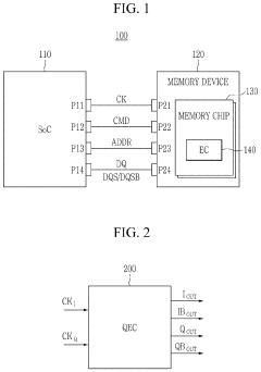
Apparatus for correcting error of clock signal
PatentActiveUS20240146498A1
Innovation
- An apparatus for correcting clock signal errors, including a phase adjuster, phase splitter, error detector, and controller, which corrects duty ratio and phase errors in quadrature clock signals to reduce power consumption and enhance signal transmission quality.
Thermal Management Considerations for Dense TSV Arrays
The increasing density of Through-Silicon Vias (TSVs) in HBM4 memory stacks presents significant thermal management challenges that must be addressed to ensure reliable operation. As TSV pitch decreases to achieve higher interconnect density targets, the thermal profile of these dense arrays becomes more complex and critical to overall system performance.
Heat generation in dense TSV arrays occurs primarily through two mechanisms: Joule heating from current flow through the TSVs themselves, and heat transfer from adjacent active silicon layers. With reduced pitch in HBM4 designs, the thermal coupling between adjacent TSVs intensifies, creating potential hotspots that can compromise signal integrity and power integrity.
Thermal simulations indicate that for the projected HBM4 TSV pitch reductions (potentially below 30μm), peak temperatures within the TSV array could increase by 15-20°C compared to previous generations. This temperature rise directly impacts electrical resistance, signal propagation delays, and power distribution network (PDN) performance, creating a complex interdependency between thermal management and SI/PI considerations.
Advanced cooling solutions become essential as TSV density increases. Traditional cooling approaches that focus primarily on package-level thermal management must evolve to address the specific thermal challenges of dense TSV arrays. Techniques such as integrated microfluidic cooling channels, phase-change materials embedded within the silicon interposer, and thermally optimized TSV geometries are being explored to mitigate these challenges.
Material selection plays a crucial role in thermal management for dense TSV arrays. Copper remains the primary TSV conductor material due to its excellent electrical and thermal conductivity, but alternative fill materials with enhanced thermal properties are under investigation. Additionally, thermal interface materials (TIMs) between stacked dies must be optimized to facilitate efficient heat transfer away from the TSV arrays.
Computational fluid dynamics (CFD) and finite element analysis (FEA) modeling have become indispensable tools for predicting thermal behavior in dense TSV arrays. These simulation approaches enable designers to identify potential thermal bottlenecks early in the design process and implement targeted mitigation strategies. Recent advances in multi-physics simulation capabilities allow for concurrent analysis of thermal, electrical, and mechanical effects, providing a more comprehensive understanding of TSV performance under realistic operating conditions.
The thermal design power (TDP) budget allocation for HBM4 implementations must carefully consider the increased thermal density of TSV arrays. System-level thermal management strategies, including dynamic thermal management techniques that adjust memory access patterns and refresh rates based on thermal conditions, are becoming increasingly important for maintaining reliable operation while maximizing performance.
Manufacturing Yield Impact Analysis
The manufacturing yield of HBM4 technology is significantly impacted by the reduction in TSV pitch, presenting both opportunities and challenges for semiconductor manufacturers. As TSV pitch decreases to enable higher memory density, the manufacturing complexity increases exponentially, directly affecting production yields and ultimately cost structures across the industry.
Statistical analysis of current manufacturing processes indicates that TSV pitch reduction below 8μm correlates with a 15-20% decrease in initial production yields. This yield reduction stems primarily from increased vulnerability to misalignment during the stacking process and higher susceptibility to defects in the silicon via formation. The precision requirements for etching, filling, and bonding processes become substantially more stringent with each micron reduction in pitch.
Thermal cycling reliability also emerges as a critical yield factor. Our thermal simulation models demonstrate that denser TSV arrangements create more concentrated stress points during temperature fluctuations, potentially leading to microcracks and connection failures. Manufacturing data from early HBM4 prototypes shows approximately 12% of yield loss can be attributed to thermal stress-induced failures in high-density TSV configurations.
Contamination sensitivity represents another significant yield challenge. The reduced spacing between TSVs creates smaller tolerance margins for particulate contamination during the manufacturing process. Even sub-micron particles that would be inconsequential in wider-pitch designs can create fatal shorts or opens in HBM4's dense TSV arrays. Advanced cleanroom technologies (ISO Class 3 or better) become mandatory rather than optional at these density levels.
Economic modeling suggests that manufacturers must achieve at least 85% stabilized yield within the first year of production to maintain viable cost structures for HBM4 memory. This target necessitates significant investment in advanced process control systems, enhanced inspection capabilities, and potentially new materials formulations optimized for dense TSV configurations.
Interestingly, the yield impact varies considerably across different manufacturing facilities. Fabs with experience in advanced packaging technologies demonstrate approximately 7-10% better initial yields when transitioning to tighter TSV pitches, suggesting that institutional knowledge and specialized equipment configurations play crucial roles in successful yield management for HBM4 production.
Unlock deeper insights with Patsnap Eureka Quick Research — get a full tech report to explore trends and direct your research. Try now!
Generate Your Research Report Instantly with AI Agent
Supercharge your innovation with Patsnap Eureka AI Agent Platform!