

How Chiplet Integration Governs Semiconductor Market Dynamics
OCT 15, 20259 MIN READ
Generate Your Research Report Instantly with AI Agent
PatSnap Eureka helps you evaluate technical feasibility & market potential.
Chiplet Technology Evolution and Objectives
Chiplet technology represents a paradigm shift in semiconductor design and manufacturing, evolving from traditional monolithic integrated circuits to a more modular approach. This evolution began in the early 2010s when semiconductor manufacturers faced increasing challenges with Moore's Law, which predicted the doubling of transistor density approximately every two years. As process nodes shrank below 10nm, the technical difficulties and costs associated with manufacturing large, complex dies grew exponentially, prompting the industry to seek alternative approaches.
The chiplet concept emerged as a solution to these challenges by disaggregating large system-on-chip (SoC) designs into smaller, more manageable functional blocks that could be manufactured separately and then integrated using advanced packaging technologies. This approach allows manufacturers to optimize each chiplet for specific functions while using the most appropriate process node for each component, balancing performance, power efficiency, and cost considerations.
A significant milestone in chiplet evolution was AMD's introduction of its Infinity Fabric interconnect technology in 2017, which enabled the company's multi-chip module (MCM) approach in its Ryzen and EPYC processors. Intel followed with its Embedded Multi-die Interconnect Bridge (EMIB) and later Foveros 3D packaging technologies, while TSMC developed its Integrated Fan-Out (InFO) and System on Integrated Chips (SoIC) technologies to facilitate chiplet integration.
The primary objectives of chiplet technology development include overcoming the physical and economic limitations of monolithic chip scaling, improving manufacturing yields by working with smaller die sizes, enabling heterogeneous integration of components manufactured using different process technologies, and accelerating time-to-market by allowing parallel development of different functional blocks.
Industry standardization efforts have become increasingly important as chiplet adoption grows. Initiatives like the Universal Chiplet Interconnect Express (UCIe) consortium, formed in 2022 with members including Intel, AMD, Arm, TSMC, and Samsung, aim to establish open interconnect standards that would allow chiplets from different vendors to work together seamlessly, potentially creating a more diverse and competitive chiplet ecosystem.
Looking forward, chiplet technology aims to enable more complex heterogeneous integration, incorporating not just different types of processors but also memory, analog components, photonics, and even non-silicon technologies. The ultimate goal is to create a "chiplet marketplace" where standardized functional blocks can be mixed and matched to create custom solutions for specific applications, fundamentally changing how semiconductor products are designed, manufactured, and brought to market.
Market Demand Analysis for Chiplet-Based Solutions
The chiplet market is experiencing unprecedented growth, driven by the increasing demand for high-performance computing solutions across various industries. Current market analysis indicates that the global chiplet market is projected to grow at a compound annual growth rate of over 40% from 2023 to 2030, reflecting the strong demand for modular semiconductor solutions that can overcome the limitations of traditional monolithic designs.
This surge in demand is primarily fueled by data centers and cloud service providers seeking more efficient and scalable computing architectures. These sectors require solutions that can deliver higher performance while managing thermal constraints and power consumption—challenges that chiplet-based designs effectively address. The hyperscaler market segment alone is expected to account for approximately 45% of chiplet adoption in the near term.
Consumer electronics represents another significant market driver, with smartphone manufacturers and personal computing device makers exploring chiplet integration to enhance product capabilities while maintaining competitive price points. This segment values the ability of chiplet technology to enable customization and differentiation in increasingly commoditized markets.
Automotive and industrial applications are emerging as high-growth segments for chiplet technology. Advanced driver-assistance systems (ADAS), autonomous vehicles, and industrial automation require sophisticated computing capabilities that can be efficiently delivered through chiplet-based architectures. The automotive semiconductor market's shift toward chiplet solutions is expected to accelerate as vehicle electrification and autonomy features become more prevalent.
Geographic market analysis reveals that North America currently leads chiplet adoption, followed closely by East Asia, particularly Taiwan, South Korea, and Japan. China is investing heavily to develop domestic chiplet capabilities as part of its semiconductor self-sufficiency strategy, while Europe is focusing on chiplet applications for automotive and industrial markets.
Customer requirements analysis shows that performance-per-watt metrics are paramount for data center applications, while cost-effectiveness and reliability dominate considerations in consumer electronics. The automotive sector emphasizes functional safety and long-term reliability, creating a diverse set of market requirements that chiplet technology must address.
Market barriers include concerns about standardization, with potential customers hesitant to commit to proprietary chiplet interfaces. The industry is responding through initiatives like Universal Chiplet Interconnect Express (UCIe) to establish common standards, which is expected to accelerate market adoption by reducing integration risks and ensuring interoperability between chiplets from different vendors.
Current Chiplet Integration Challenges and Limitations
Despite the promising advancements in chiplet technology, significant technical challenges and limitations continue to impede widespread adoption and optimal implementation. The primary obstacle remains the interconnect technology between chiplets. Current approaches like silicon interposers and organic substrates face trade-offs between performance, power efficiency, and manufacturing complexity. Silicon interposers offer excellent electrical characteristics but are expensive and difficult to manufacture at scale, while organic substrates are more cost-effective but compromise on signal integrity and bandwidth.
Thermal management presents another critical challenge as chiplets from different process nodes and manufacturers generate varying heat profiles. The heterogeneous nature of chiplet designs creates hotspots and thermal gradients that conventional cooling solutions struggle to address effectively. This issue becomes particularly pronounced in high-performance computing applications where thermal constraints can significantly limit system performance.
Testing and validation methodologies for chiplet-based systems remain underdeveloped. Traditional testing approaches designed for monolithic chips are inadequate for multi-chiplet architectures, creating difficulties in identifying defects at the die-to-die interfaces. Known-good-die testing becomes exponentially more complex when dealing with multiple chiplets from different vendors, leading to yield and reliability concerns.
The lack of standardization across the industry represents a substantial barrier to chiplet ecosystem development. Despite initiatives like UCIe (Universal Chiplet Interconnect Express), the industry still lacks comprehensive standards for chiplet interfaces, protocols, and physical dimensions. This fragmentation hinders interoperability between chiplets from different vendors and increases integration complexity.
Supply chain coordination introduces additional complications as chiplet-based designs require synchronized production across multiple suppliers. Delays or quality issues from any single supplier can disrupt the entire manufacturing process. This interdependence creates new vulnerabilities in the semiconductor supply chain that don't exist in traditional monolithic chip production.
Design tools and methodologies for chiplet-based systems remain immature. EDA (Electronic Design Automation) tools optimized for monolithic designs lack sophisticated capabilities for modeling die-to-die interfaces, system-level power distribution, and multi-physics simulations across heterogeneous chiplets. This tooling gap increases design complexity and time-to-market.
Intellectual property protection and business models present non-technical but equally significant challenges. The collaborative nature of chiplet-based designs raises questions about IP ownership, licensing models, and liability for system-level failures. These unresolved issues create hesitation among potential ecosystem participants and slow market development.
Current Chiplet Integration Methodologies
01 Advanced Packaging Technologies for Chiplet Integration
Advanced packaging technologies are crucial for chiplet integration, enabling multiple dies to be combined into a single package. These technologies include 2.5D and 3D integration methods, interposer-based solutions, and fan-out wafer-level packaging. These approaches allow for higher performance, reduced power consumption, and improved thermal management in multi-die systems, driving the chiplet integration market forward.- Advanced Packaging Technologies for Chiplet Integration: Advanced packaging technologies are crucial for chiplet integration, enabling multiple dies to be combined into a single package. These technologies include 2.5D and 3D integration methods, interposer-based solutions, and fan-out wafer-level packaging. Such approaches allow for heterogeneous integration of chiplets with different functionalities, process nodes, or from different manufacturers, creating more powerful and efficient semiconductor devices while overcoming the limitations of monolithic integration.
- Interconnect Solutions for Chiplet-to-Chiplet Communication: Efficient interconnect solutions are essential for enabling high-bandwidth, low-latency communication between chiplets. These include advanced die-to-die interfaces, silicon bridges, through-silicon vias (TSVs), and microbumps. The development of standardized interconnect protocols and architectures facilitates interoperability between chiplets from different vendors, addressing one of the key challenges in the chiplet ecosystem and enabling more flexible system design and integration.
- Market Trends and Economic Factors in Chiplet Adoption: The chiplet integration market is influenced by various economic factors and industry trends. These include the rising costs of advanced node manufacturing, increasing demand for specialized computing solutions, supply chain considerations, and the need for more flexible product development cycles. Chiplet-based designs offer cost advantages by allowing manufacturers to mix and match different process nodes, reuse proven IP blocks, and potentially improve yield rates compared to large monolithic dies.
- Thermal Management and Power Optimization for Chiplet Designs: Thermal management and power optimization are critical challenges in chiplet integration. The dense packaging of multiple dies creates hotspots and thermal gradients that must be managed effectively. Advanced cooling solutions, thermal interface materials, and power delivery networks are being developed specifically for chiplet architectures. Additionally, power management techniques such as dynamic voltage and frequency scaling across different chiplets help optimize overall system efficiency while maintaining performance targets.
- Design Tools and Methodologies for Chiplet-Based Systems: Specialized design tools and methodologies are emerging to address the unique challenges of chiplet-based system development. These include advanced EDA tools for multi-die planning and verification, physical design automation for heterogeneous integration, and test methodologies for known-good-die selection. Additionally, new simulation capabilities are being developed to model the electrical, thermal, and mechanical interactions between chiplets in a package, enabling more accurate performance predictions and reliability assessments.
02 Interconnect Solutions for Chiplet-to-Chiplet Communication
Efficient interconnect technologies are essential for communication between chiplets in integrated systems. These include high-bandwidth die-to-die interfaces, silicon bridges, and advanced I/O protocols that enable seamless data transfer between different functional blocks. The development of standardized interconnect solutions is helping to address interoperability challenges and accelerate market adoption of chiplet-based designs.Expand Specific Solutions03 Design and Testing Methodologies for Heterogeneous Integration
Specialized design and testing methodologies are being developed to address the unique challenges of heterogeneous chiplet integration. These include new EDA tools for multi-die systems, design-for-test approaches for chiplet interfaces, and verification techniques for ensuring proper functionality across chiplet boundaries. These methodologies are critical for reducing development time and ensuring reliability in complex chiplet-based products.Expand Specific Solutions04 Manufacturing and Supply Chain Innovations
The chiplet integration market is driving innovations in manufacturing processes and supply chain management. This includes advancements in die preparation, handling, and placement technologies, as well as new approaches to known-good-die testing and yield management. The disaggregation of semiconductor manufacturing enabled by chiplets is creating new business models and partnership opportunities across the semiconductor ecosystem.Expand Specific Solutions05 Market Trends and Business Models for Chiplet Ecosystems
The chiplet integration market is evolving with new business models and ecosystem approaches. This includes the development of chiplet marketplaces, IP licensing strategies, and standardization efforts to enable multi-vendor chiplet integration. Market dynamics are being shaped by factors such as cost optimization, performance requirements, and the need for specialized functionality in applications ranging from high-performance computing to edge AI devices.Expand Specific Solutions
Key Semiconductor Players in Chiplet Ecosystem
The chiplet integration market is currently in a growth phase, characterized by increasing adoption across semiconductor sectors. Market dynamics reveal a competitive landscape dominated by established players like TSMC, Samsung, and Intel, who are leveraging their manufacturing capabilities to advance chiplet technologies. The market size is expanding rapidly, projected to reach significant valuation as chiplet-based designs address scaling challenges in traditional monolithic approaches. From a technical maturity perspective, the industry shows varied development stages: TSMC leads with advanced packaging solutions, IBM demonstrates research strength in heterogeneous integration, while Intel pursues its advanced packaging roadmap. Academic institutions like Fudan University and National Yang Ming Chiao Tung University contribute valuable research, creating a collaborative ecosystem between industry and academia that drives innovation in this transformative semiconductor approach.
Taiwan Semiconductor Manufacturing Co., Ltd.
Technical Solution: TSMC has pioneered advanced chiplet integration through their CoWoS (Chip-on-Wafer-on-Substrate) and InFO (Integrated Fan-Out) packaging technologies. Their CoWoS platform enables the integration of multiple silicon dies on a silicon interposer with through-silicon vias (TSVs), facilitating high-bandwidth, low-latency connections between chiplets. TSMC's 3DFabric technology portfolio further extends their chiplet capabilities, offering SOIC (System on Integrated Chips) that combines chiplet and advanced packaging technologies. Their latest advancements include the 3DFabric Alliance, an open ecosystem initiative that brings together EDA, memory, IP, and testing partners to accelerate chiplet-based designs. TSMC has demonstrated performance improvements of up to 15% and power reductions of approximately 25% when implementing chiplet designs compared to monolithic approaches in certain applications.
Strengths: Industry-leading process nodes give TSMC significant advantages in chiplet manufacturing; extensive ecosystem partnerships enable comprehensive solutions; proven high-volume manufacturing capabilities. Weaknesses: Higher costs compared to traditional packaging; intellectual property dependencies with partners can complicate implementation; thermal management challenges in densely packed chiplet designs.
Invensas Bonding Technologies, Inc.
Technical Solution: Invensas, a subsidiary of Xperi Corporation, has developed advanced chiplet integration technologies focused on direct bond interconnect (DBI) and hybrid bonding solutions. Their DBI Ultra technology enables fine-pitch, high-density connections between chiplets with bond pitches below 10 microns, significantly exceeding the capabilities of traditional micro-bump approaches. Invensas' ZiBond technology provides room-temperature covalent bonding that creates oxide-to-oxide bonds without requiring additional materials, enabling wafer-to-wafer and die-to-wafer stacking with excellent mechanical strength. Their hybrid bonding approach combines dielectric bonding with metal-to-metal connections, achieving electrical interconnects with lower resistance and parasitic capacitance compared to traditional approaches. Research data shows that Invensas' technologies can achieve up to 100x higher interconnect densities than conventional packaging methods, while reducing power consumption by approximately 20-30% in high-bandwidth applications. Their technologies have been licensed to major semiconductor manufacturers for applications ranging from high-performance computing to mobile processors.
Strengths: Industry-leading bond pitch capabilities enable ultra-high-density chiplet integration; room-temperature bonding processes reduce thermal stress; strong intellectual property portfolio with numerous patents. Weaknesses: Relies on licensing business model rather than manufacturing; requires specialized equipment and processes; higher initial implementation costs compared to conventional packaging approaches.
Core Chiplet Interconnect Technologies and Patents
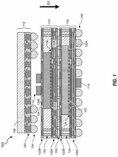
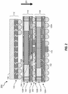
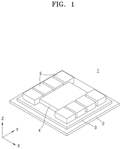
3D chiplet integration using fan-out wafer-level packaging
PatentPendingUS20240274587A1
Innovation
- The use of fan-out wafer-level packaging and three-dimensional packaging techniques for combining semiconductor chips and embedded memory in configurations such as face-to-back, back-to-back, and face-to-face orientations, enabling direct connections between chiplets and reducing assembly package sizes and manufacturing complexity.
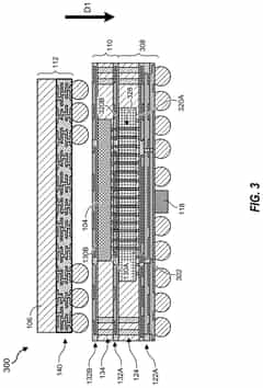
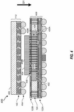
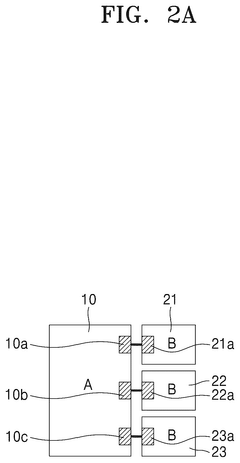
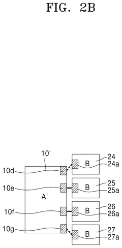
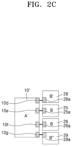
Semiconductor device
PatentPendingUS20250293165A1
Innovation
- A semiconductor device with configurable chiplet dies and an interposer, featuring a die-to-die interface with adjustable modules and a selection circuit that allows for variable alignment of connection modules, enabling efficient inter-chiplet communication without the need for new chiplet designs.
Supply Chain Implications of Chiplet Adoption
The adoption of chiplet technology is fundamentally reshaping semiconductor supply chains, creating both opportunities and challenges across the ecosystem. Traditional monolithic chip production relied on vertically integrated supply chains dominated by IDMs (Integrated Device Manufacturers). However, chiplet architecture enables a more modular approach, allowing specialized suppliers to focus on specific components that can be integrated through advanced packaging technologies.
This shift towards disaggregation is creating new specialized market segments within the semiconductor value chain. Packaging and integration services are experiencing unprecedented growth as they become critical enablers of chiplet-based designs. Companies with advanced packaging capabilities like TSMC, Intel, and ASE are strategically positioning themselves as integration hubs in this evolving landscape.
Material suppliers are also adapting to meet the demands of chiplet integration, particularly for advanced substrates, interposers, and specialized bonding materials. The increased complexity of these components has elevated their strategic importance in the supply chain, creating new value capture opportunities for materials specialists.
Testing methodologies are evolving significantly to address the unique challenges of chiplet designs. Known-good-die testing has become essential to ensure individual chiplets function properly before integration, preventing costly failures in final assemblies. This has spurred innovation in testing equipment and methodologies, creating new market opportunities for testing solution providers.
Geographic diversification presents another critical dimension of chiplet supply chain implications. While advanced node fabrication remains concentrated in East Asia, chiplet technology potentially enables more distributed manufacturing models. Different components can be produced in various regions based on comparative advantages, potentially reducing geopolitical risks and creating more resilient supply networks.
Inventory management practices are also transforming as chiplet adoption increases. The modular nature of chiplets allows for more flexible production planning and potentially reduced lead times for certain applications. However, it also introduces new coordination challenges across multiple suppliers and integration partners.
Intellectual property management has become increasingly complex in chiplet ecosystems. Standards for chiplet interfaces and integration protocols are emerging as critical factors for supply chain efficiency. Organizations like the Universal Chiplet Interconnect Express (UCIe) consortium are working to establish common frameworks that could significantly impact how value is distributed across the supply chain.
Standardization Efforts in Chiplet Interfaces
The standardization of chiplet interfaces represents a critical inflection point in the semiconductor industry's evolution toward disaggregated chip designs. As chiplet technology gains momentum, the lack of universal standards has emerged as a significant barrier to widespread adoption and market growth. Several industry consortia and leading companies have initiated standardization efforts to address this challenge, with the Universal Chiplet Interconnect Express (UCIe) emerging as a prominent framework since its introduction in 2022.
UCIe, backed by industry giants including Intel, AMD, Arm, TSMC, and Samsung, aims to establish an open specification for die-to-die interconnection. This standard focuses on both the physical layer and protocol stack, enabling chiplets from different vendors to communicate seamlessly when integrated into a single package. The specification covers critical aspects such as electrical parameters, physical design considerations, and communication protocols that ensure interoperability.
Parallel to UCIe, other notable standardization initiatives include JEDEC's Chiplet Physical Interface (CXL), Advanced Interface Bus (AIB) by Intel, and Open Compute Project's Bunch of Wires (BoW) specification. Each of these standards addresses specific aspects of chiplet integration, from high-bandwidth communication to power efficiency and manufacturing considerations.
The economic implications of these standardization efforts are profound. By establishing common interfaces, the industry can potentially transform from a vertically integrated model to a more horizontally specialized ecosystem. This shift would enable smaller players to focus on developing specialized chiplets without needing to master the entire system integration process, thereby lowering barriers to entry and fostering innovation.
Market analysts project that successful standardization could accelerate chiplet adoption by 30-40% over the next five years, potentially creating a specialized chiplet market worth $5-7 billion by 2027. Companies that actively participate in shaping these standards gain strategic advantages in terms of intellectual property positioning and market influence.
Technical challenges in standardization include balancing performance requirements with backward compatibility, addressing thermal management concerns across heterogeneous components, and ensuring security in multi-vendor chiplet environments. The resolution of these challenges will significantly influence market dynamics, determining which companies and regions gain competitive advantages in the next generation of semiconductor design and manufacturing.
Unlock deeper insights with PatSnap Eureka Quick Research — get a full tech report to explore trends and direct your research. Try now!
Generate Your Research Report Instantly with AI Agent
Supercharge your innovation with PatSnap Eureka AI Agent Platform!