How Do GaN HEMTs Compare To Next-Generation Power Devices?
SEP 8, 20259 MIN READ
Generate Your Research Report Instantly with AI Agent
Patsnap Eureka helps you evaluate technical feasibility & market potential.
GaN HEMT Technology Evolution and Objectives
Gallium Nitride High Electron Mobility Transistors (GaN HEMTs) have emerged as revolutionary power semiconductor devices since their initial development in the early 1990s. The evolution of GaN technology has been characterized by significant breakthroughs in material science, device architecture, and manufacturing processes. Initially developed for RF applications in defense and telecommunications, GaN HEMTs have progressively expanded into power electronics domains due to their superior performance characteristics compared to traditional silicon-based devices.
The technological trajectory of GaN HEMTs has been marked by several pivotal advancements. The early 2000s witnessed the first commercial GaN-on-Silicon devices, which dramatically reduced production costs compared to GaN-on-SiC or GaN-on-sapphire alternatives. By 2010, enhanced passivation techniques and field plate structures significantly improved device reliability and breakdown voltage capabilities, enabling higher voltage applications. The period between 2015 and 2020 saw substantial progress in reducing dynamic on-resistance and current collapse phenomena, which had previously limited GaN's practical implementation in power conversion systems.
Current GaN HEMT technology has achieved remarkable performance metrics, including switching frequencies exceeding 100 MHz, power densities above 5 W/mm², and efficiencies surpassing 99% in certain applications. These capabilities have positioned GaN as a formidable competitor to both silicon-based power devices and emerging wide bandgap alternatives such as silicon carbide (SiC).
The primary objectives driving GaN HEMT development focus on several key areas. First is the continuous enhancement of reliability and robustness, particularly addressing challenges related to gate leakage current and threshold voltage stability under high-temperature operation. Second is cost reduction through improved manufacturing yields and innovative packaging solutions that can effectively manage GaN's unique thermal characteristics. Third is the development of higher voltage capabilities, with research targeting 1200V and beyond to compete directly with SiC in medium to high-voltage applications.
Looking forward, the GaN HEMT technology roadmap aims to achieve vertical device architectures that could potentially offer even higher breakdown voltages while maintaining the exceptional switching performance of lateral devices. Integration capabilities are another critical objective, with significant research directed toward monolithic integration of gate drivers and protection circuits to create more compact and efficient power modules.
The ultimate goal for GaN HEMT technology is to establish a comprehensive ecosystem that enables seamless adoption across diverse applications, from consumer electronics and automotive systems to industrial power conversion and renewable energy infrastructure, thereby accelerating the transition from silicon-based power devices to more efficient wide bandgap solutions.
Power Electronics Market Demand Analysis
The global power electronics market is experiencing robust growth, driven by increasing electrification across multiple sectors. Current market valuations place the power electronics industry at approximately $40 billion, with projections indicating a compound annual growth rate (CAGR) of 4.7% through 2028. This growth trajectory is particularly significant for wide bandgap (WBG) semiconductor devices, where GaN HEMTs are positioned as key technological enablers.
Electric vehicle (EV) adoption represents one of the strongest demand drivers for advanced power devices. With global EV sales growing at over 35% annually, the need for efficient power conversion solutions has intensified. GaN HEMTs, with their superior switching speeds and reduced power losses, directly address the automotive industry's requirements for extending vehicle range through more efficient power management systems.
Renewable energy integration presents another substantial market opportunity. The solar inverter market alone is expected to reach $27 billion by 2026, with increasing pressure to improve efficiency and reduce form factors. GaN-based power devices offer significant advantages in these applications, potentially increasing conversion efficiency by 2-3 percentage points compared to silicon alternatives while reducing system size by up to 40%.
Data center power infrastructure represents a rapidly expanding application area for next-generation power devices. With global data center electricity consumption approaching 3% of worldwide usage, the industry faces mounting pressure to improve energy efficiency. GaN HEMTs enable higher frequency operation in power supplies, resulting in smaller passive components and improved power density—critical factors as rack power densities continue to increase.
Consumer electronics manufacturers are increasingly adopting GaN technology for fast-charging applications. The mobile device fast-charging market is growing at 20% annually, with consumers demanding ever-shorter charging times. GaN-based chargers deliver up to 3x faster charging while reducing adapter size by up to 60% compared to silicon solutions.
Industrial automation systems represent another significant market segment, with demands for more compact motor drives and power supplies. The industrial power electronics market segment is projected to grow at 5.3% CAGR, with particular emphasis on improved reliability and efficiency in harsh operating environments—areas where GaN HEMTs demonstrate clear advantages.
Regional analysis reveals Asia-Pacific as the dominant manufacturing hub for power electronics, accounting for over 60% of global production. However, recent supply chain disruptions have accelerated efforts to diversify manufacturing locations, with significant investments in North American and European production facilities for advanced semiconductor technologies including GaN.
Current State and Challenges of Wide Bandgap Semiconductors
Wide bandgap (WBG) semiconductors represent a significant advancement in power electronics, with materials such as Silicon Carbide (SiC) and Gallium Nitride (GaN) leading the technological frontier. These materials offer superior properties compared to conventional silicon, including higher breakdown voltage, faster switching speeds, and better thermal conductivity, making them ideal for high-power and high-frequency applications.
The global market for WBG semiconductors is experiencing robust growth, projected to reach $4.5 billion by 2025, with a compound annual growth rate exceeding 25%. This expansion is primarily driven by increasing demands in electric vehicles, renewable energy systems, and industrial power conversion applications where efficiency and power density are paramount.
Despite their promising characteristics, WBG semiconductors face several significant challenges. Material quality remains a critical issue, with defect densities in GaN and SiC substrates still higher than those in silicon, affecting device reliability and yield. The epitaxial growth of GaN on foreign substrates like silicon or silicon carbide introduces additional complexities due to lattice mismatch and thermal expansion coefficient differences.
Manufacturing scalability presents another major hurdle. Current production processes for WBG materials are more complex and costly than silicon manufacturing, resulting in higher device prices that limit widespread adoption. The industry is actively working to develop more cost-effective fabrication techniques and increase wafer sizes to achieve economies of scale.
Device design and packaging technologies specifically optimized for WBG semiconductors are still evolving. The high-frequency operation capabilities of GaN HEMTs, for instance, require advanced packaging solutions to minimize parasitic inductances and capacitances that can degrade performance. Similarly, thermal management becomes increasingly critical as these devices operate at higher power densities.
Reliability and qualification standards for WBG devices are still maturing. Long-term stability under various operating conditions, particularly at elevated temperatures and high electric fields, remains an area of ongoing research. The industry is working to establish standardized testing protocols and reliability models specific to WBG technologies.
Geographically, WBG semiconductor development shows distinct patterns. The United States leads in GaN research and commercialization, with significant contributions from companies like Wolfspeed, GaN Systems, and academic institutions. Japan dominates in SiC technology, while European research centers focus on both materials with emphasis on automotive applications. China has made substantial investments to build domestic capabilities in WBG semiconductor manufacturing, aiming to reduce dependency on imports for these strategic technologies.
Comparative Analysis of Power Device Solutions
01 Device structure optimization for GaN HEMTs
Various structural modifications can enhance GaN HEMT performance. These include optimized gate designs, buffer layer engineering, and novel channel configurations. Improved device structures lead to better electron mobility, reduced leakage currents, and enhanced thermal management. These optimizations directly impact key performance metrics such as breakdown voltage, on-resistance, and switching speed.- Device structure optimization for GaN HEMTs: Various structural optimizations in GaN HEMTs can significantly enhance performance metrics. These include modifications to the gate structure, buffer layer design, and channel engineering. Advanced gate designs like recessed gates or field plates help manage electric fields and reduce leakage current. Optimized buffer layers improve carrier confinement and reduce trapping effects, while channel engineering techniques enhance electron mobility and current density. These structural improvements collectively lead to better power handling capability and frequency response.
- Material composition and epitaxial growth techniques: The performance of GaN HEMTs is heavily influenced by material composition and epitaxial growth methods. Different barrier materials such as AlGaN, InAlN, or AlN can be used to create the 2DEG channel with varying electron densities and mobilities. Advanced epitaxial growth techniques like MOCVD or MBE with precise control over layer thickness and composition uniformity result in higher quality heterostructures. Innovations in substrate materials and buffer layer compositions help mitigate lattice mismatch issues and reduce defect densities, leading to improved device reliability and performance.
- Thermal management and reliability enhancements: Thermal management is critical for GaN HEMT performance and reliability. Various approaches include substrate material selection (SiC, diamond), improved heat dissipation structures, and novel packaging techniques. Advanced thermal management solutions help maintain lower junction temperatures during high-power operation, reducing performance degradation. Reliability enhancements focus on mitigating degradation mechanisms like current collapse and electron trapping through surface passivation techniques, field plate optimization, and buffer layer engineering. These improvements extend device lifetime and maintain stable performance under harsh operating conditions.
- High-frequency and power performance optimization: GaN HEMTs can be optimized for either high-frequency operation or power handling capability through specific design considerations. For high-frequency performance, shorter gate lengths, reduced parasitic capacitances, and optimized access regions improve cutoff frequencies and gain. Power performance optimization involves increasing breakdown voltage through field management techniques, enhancing current density with channel engineering, and improving thermal dissipation. Comparative analyses show that GaN HEMTs significantly outperform conventional silicon-based transistors in terms of power density, efficiency, and frequency response in RF and power applications.
- Novel GaN HEMT architectures and integration techniques: Innovative GaN HEMT architectures are being developed to push performance boundaries. These include enhancement-mode (normally-off) configurations using various gate technologies, vertical device structures for higher voltage handling, and multi-channel designs for increased current capacity. Integration techniques focus on monolithic integration with other semiconductor technologies, enabling advanced power management circuits and RF systems. Hybrid and heterogeneous integration approaches combine GaN HEMTs with silicon CMOS or other III-V devices to create high-performance systems that leverage the advantages of each technology while addressing their individual limitations.
02 Material composition and substrate innovations
The performance of GaN HEMTs is significantly influenced by material composition and substrate selection. Advanced epitaxial growth techniques and novel substrate materials like silicon carbide or diamond improve thermal conductivity and reduce lattice mismatch. Innovations in barrier layers, such as AlGaN/GaN heterostructures with optimized aluminum content, enhance carrier concentration and mobility in the two-dimensional electron gas (2DEG) region.Expand Specific Solutions03 Power efficiency and high-frequency performance
GaN HEMTs demonstrate superior power efficiency and high-frequency performance compared to silicon-based transistors. Performance comparisons show advantages in power density, efficiency at high frequencies, and operation at elevated temperatures. Enhanced electron saturation velocity and higher breakdown field strength enable GaN HEMTs to operate efficiently in power conversion applications and RF amplifiers, with reduced switching losses and improved power-added efficiency.Expand Specific Solutions04 Reliability and thermal management solutions
Reliability challenges in GaN HEMTs include current collapse, dynamic on-resistance, and thermal degradation. Advanced thermal management solutions incorporate innovative heat dissipation structures, optimized packaging techniques, and improved die attach materials. Performance comparisons between different thermal management approaches show significant improvements in device lifetime, stability under high-power operation, and consistent performance across temperature variations.Expand Specific Solutions05 Integration and packaging technologies
Integration and packaging technologies significantly impact overall GaN HEMT system performance. Advanced packaging solutions reduce parasitic inductances and capacitances, improving switching performance and thermal management. Monolithic integration approaches enable compact power modules with enhanced functionality. Performance comparisons between different integration strategies demonstrate trade-offs between cost, size, thermal performance, and electrical characteristics in various application scenarios.Expand Specific Solutions
Key Players in GaN and Next-Gen Power Device Industry
GaN HEMT technology is currently in a growth phase, with the market expanding rapidly due to increasing demand for high-efficiency power devices. The global market for GaN power devices is projected to reach significant scale as applications in electric vehicles, 5G infrastructure, and renewable energy drive adoption. From a technical maturity perspective, key players are advancing the technology at different rates. Wolfspeed and GaN Systems lead in commercialization of GaN HEMTs, while Innoscience has emerged as a major player in silicon-based GaN technology. Traditional semiconductor companies like Texas Instruments, QUALCOMM, and Mitsubishi Electric are investing heavily in GaN R&D. Academic institutions including South China University of Technology and Xidian University contribute significant research. Compared to next-generation alternatives, GaN HEMTs offer superior high-frequency performance and power density, positioning them favorably in the evolving power semiconductor landscape.
Wolfspeed, Inc.
Technical Solution: Wolfspeed has pioneered silicon carbide (SiC) technology as a next-generation alternative to GaN HEMTs, focusing on high-power, high-frequency applications. Their SiC MOSFETs and Schottky diodes operate at higher voltages (up to 1700V) compared to typical GaN devices (650V). Wolfspeed's vertical SiC MOSFET structure offers superior thermal performance with junction-to-case thermal resistance as low as 0.15°C/W for high-current devices[1]. Their latest generation platforms achieve on-resistance values below 25mΩ at 1200V ratings, enabling power densities exceeding 100W/in³ in converter applications[3]. Wolfspeed has also developed specialized packaging solutions to maximize SiC benefits, including low-inductance modules that reduce switching losses by approximately 30% compared to conventional packages[5].
Strengths: Superior high-voltage handling capability (1200-1700V range), better thermal conductivity (3-4x that of GaN), and established manufacturing infrastructure. Weaknesses: Higher cost structure than silicon, slower switching speeds compared to GaN HEMTs, and larger die sizes required for equivalent current ratings.
GaN Systems, Inc.
Technical Solution: GaN Systems specializes in gallium nitride power transistors, focusing on high-frequency, high-efficiency applications. Their proprietary Island Technology® creates devices with significantly reduced die size (up to 4x smaller than comparable silicon devices) while maintaining high current capability[2]. Their GaN E-HEMTs operate at switching frequencies up to 10MHz, compared to silicon's typical 100kHz limit, enabling dramatic reduction in passive component sizes. GaN Systems' latest 650V platform achieves RDS(on) values as low as 7mΩ with switching losses approximately 5x lower than silicon counterparts[4]. Their thermal innovation includes GaNPX® packaging that eliminates wire bonds and provides dual-sided cooling, reducing thermal resistance by up to 50% compared to conventional packages. The company has demonstrated power densities exceeding 3kW/in³ in automotive onboard charger applications[6].
Strengths: Superior high-frequency performance (MHz range operation), extremely fast switching capability (sub-10ns rise times), and excellent power density. Weaknesses: Limited voltage range (typically ≤650V), higher cost than silicon alternatives, and relatively newer manufacturing processes with less long-term reliability data.
Critical Patents and Innovations in GaN HEMT Technology
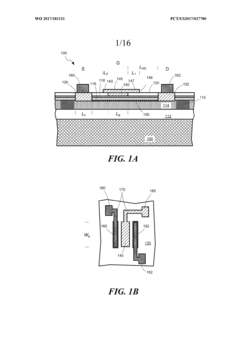
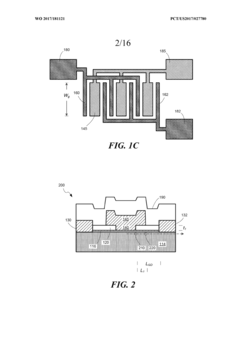
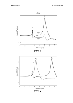
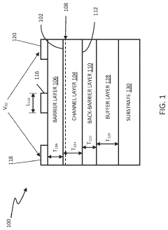
High-voltage GAN high electron mobility transistors
PatentWO2017181121A2
Innovation
- The development of high-voltage HEMTs with a gallium-nitride material structure, including a buffer layer, conduction layer, barrier layer, gate, source, and drain, with a gate-connected field plate extending beyond the gate edges, and a thin gallium-oxide layer formed through oxygen plasma treatment, to enhance reverse-bias voltage withstand and reduce leakage currents.

HIGH ELECTRON MOBILITY TRANSISTORS (HEMTS) INCLUDING A YTTRIUM (Y) AND ALUMINUM NITRIDE (AlN) (YAlN) ALLOY LAYER
PatentActiveUS20230223467A1
Innovation
- Incorporating a lattice-matched yttrium aluminum nitride (YAlN) alloy as a back-barrier layer in HEMTs, which has a wider bandgap than the gallium nitride channel layer, preventing secondary 2DEG formation and reducing thermal resistance, and can be used as an etch stop layer to improve electron confinement and gate control.
Thermal Management and Reliability Considerations
Thermal management represents a critical challenge in the deployment of GaN HEMTs for power applications. Despite GaN's superior thermal conductivity compared to silicon, the high power density operation of these devices generates significant heat that must be efficiently dissipated. Current GaN HEMT designs typically employ advanced packaging solutions including direct bonded copper (DBC) substrates and integrated heat spreaders to manage thermal loads. However, as power densities continue to increase, these conventional approaches are reaching their physical limitations.
The reliability of GaN HEMTs under thermal stress remains a key concern for widespread commercial adoption. Accelerated life testing has revealed that GaN devices can experience several degradation mechanisms under elevated temperatures, including gate sinking, ohmic contact degradation, and electron trapping phenomena. These reliability issues are particularly pronounced at the high junction temperatures that can occur during normal operation of power conversion systems.
Compared to emerging alternatives such as SiC MOSFETs, GaN HEMTs demonstrate different thermal behavior patterns. While SiC offers superior thermal conductivity (approximately 3-4 times that of GaN), GaN devices can operate at higher frequencies, which affects the thermal design considerations. This creates a complex trade-off scenario where system-level thermal management must be optimized differently depending on the selected technology.
Recent innovations in thermal management for GaN include the development of diamond heat spreaders, which leverage diamond's exceptional thermal conductivity (>2000 W/mK). Research has shown that GaN-on-diamond technology can potentially reduce the thermal resistance by up to 40% compared to conventional substrates, enabling higher power density operation without reliability compromises.
Reliability qualification standards for GaN power devices have evolved significantly, with JEDEC and AEC-Q101 standards being adapted to address the unique characteristics of wide bandgap semiconductors. Mean Time To Failure (MTTF) projections for current-generation GaN HEMTs now exceed 10^7 hours at operating temperatures of 150°C, approaching the reliability levels required for automotive applications.
The dynamic thermal response of GaN HEMTs presents another challenge, as these devices can experience significant temperature fluctuations during switching events. This thermal cycling can accelerate failure mechanisms such as die attach degradation and wire bond fatigue. Advanced modeling techniques, including electro-thermal co-simulation, have become essential tools for predicting device behavior under realistic operating conditions.
Sustainability Impact of Wide Bandgap Power Devices
The transition to wide bandgap (WBG) semiconductor materials, particularly Gallium Nitride (GaN) and Silicon Carbide (SiC), represents a significant advancement in sustainable power electronics. These materials offer substantial environmental benefits compared to traditional silicon-based devices, primarily through improved energy efficiency. GaN HEMTs (High Electron Mobility Transistors) can operate at higher frequencies with lower switching losses, resulting in power conversion efficiency improvements of 10-15% over conventional silicon technologies.
This efficiency gain translates directly into reduced energy consumption across numerous applications, from data centers to electric vehicles. Calculations indicate that widespread adoption of GaN power devices could reduce global electricity consumption by approximately 2-3% annually, equivalent to eliminating hundreds of millions of tons of CO2 emissions.
Beyond operational efficiency, WBG devices offer sustainability advantages throughout their lifecycle. The manufacturing process for GaN HEMTs requires fewer resources per unit of power handling capability compared to silicon alternatives. While GaN wafer production currently has higher energy intensity, the extended device lifespan and superior performance characteristics offset this initial environmental cost over the product lifecycle.
The compact size of GaN-based power systems reduces material requirements by 30-50% compared to silicon equivalents. This miniaturization decreases the environmental footprint associated with raw material extraction, processing, and transportation. Additionally, the higher temperature tolerance of GaN devices (operating efficiently at temperatures exceeding 200°C) reduces cooling requirements, further decreasing system-level energy consumption.
From a circular economy perspective, WBG devices present both challenges and opportunities. Their longer operational lifespan reduces replacement frequency and associated waste. However, end-of-life recycling processes for GaN and other WBG materials remain underdeveloped compared to established silicon recycling infrastructure. Research into efficient recovery methods for gallium and other critical materials from spent devices represents an important sustainability frontier.
The transition to WBG power devices also supports broader sustainability initiatives, particularly renewable energy integration. The high-frequency operation of GaN HEMTs enables more efficient power conversion in solar inverters and wind power systems, improving renewable energy economics. In electric vehicle applications, GaN-based power electronics can extend range by 5-10% through reduced power losses, accelerating transportation electrification.
Unlock deeper insights with Patsnap Eureka Quick Research — get a full tech report to explore trends and direct your research. Try now!
Generate Your Research Report Instantly with AI Agent
Supercharge your innovation with Patsnap Eureka AI Agent Platform!