How is Chiplet Integration Affecting the Semiconductor Industry
OCT 15, 20259 MIN READ
Generate Your Research Report Instantly with AI Agent
Patsnap Eureka helps you evaluate technical feasibility & market potential.
Chiplet Technology Evolution and Objectives
Chiplet technology represents a paradigm shift in semiconductor design and manufacturing, evolving from the traditional monolithic system-on-chip (SoC) approach to a more modular architecture. This evolution began in the early 2010s as semiconductor manufacturers faced increasing challenges with Moore's Law, which had guided industry progress for decades. The physical limitations of silicon scaling, coupled with exponentially rising costs of advanced process nodes, necessitated a fundamental rethinking of chip design methodologies.
The evolution of chiplet technology can be traced through several key phases. Initially, multi-chip modules (MCMs) in the 1990s and 2000s provided a foundation for the concept of combining multiple silicon dies in a single package. By 2015-2017, companies like AMD pioneered commercial chiplet implementations with their Zen architecture, demonstrating the viability of disaggregated designs for high-performance computing applications.
Between 2018 and 2020, the industry witnessed rapid advancement in integration technologies, including enhanced interposer designs, advanced packaging solutions like EMIB (Embedded Multi-die Interconnect Bridge) from Intel, and CoWoS (Chip-on-Wafer-on-Substrate) from TSMC. These developments significantly improved die-to-die communication bandwidth while reducing power consumption and latency penalties.
The primary objective of chiplet technology is to overcome the economic and technical barriers of monolithic chip scaling. By disaggregating complex SoCs into smaller, specialized dies manufactured using optimal process nodes, chiplet architecture enables continued performance scaling while managing manufacturing costs and improving yields. This approach allows semiconductor companies to mix and match different process technologies, optimizing each component for its specific function rather than compromising on a single process for the entire chip.
Another critical objective is enhancing design flexibility and reusability. Chiplets enable a more modular approach to semiconductor design, where pre-validated functional blocks can be reused across multiple products, significantly reducing development time and engineering costs. This modular approach also facilitates more rapid innovation cycles, as individual components can be upgraded independently without redesigning the entire system.
Looking forward, the industry aims to establish standardized chiplet interfaces and ecosystems that would enable true interoperability between chiplets from different vendors. Initiatives like the Universal Chiplet Interconnect Express (UCIe) consortium represent significant steps toward creating an open chiplet marketplace, which could fundamentally transform the semiconductor value chain and enable new business models based on specialized chiplet design and integration services.
Market Demand Analysis for Chiplet Solutions
The global chiplet market is experiencing unprecedented growth, driven by the increasing demand for high-performance computing solutions across various industries. Current market projections indicate the chiplet market will reach approximately $5.8 billion by 2024, with a compound annual growth rate exceeding 40% through 2028. This remarkable expansion is primarily fueled by the semiconductor industry's transition away from traditional monolithic designs toward more modular and efficient architectures.
Data centers and cloud service providers represent the largest market segment for chiplet technology, accounting for nearly 45% of current demand. These entities require increasingly powerful processors to handle artificial intelligence workloads, big data analytics, and virtualization services. The chiplet approach allows them to deploy customized solutions with optimized performance-per-watt metrics, addressing both computational needs and energy efficiency concerns.
Consumer electronics manufacturers constitute the second-largest market segment, particularly smartphone and personal computing device producers seeking enhanced performance within strict power and thermal constraints. Market research indicates that approximately 30% of high-end smartphones will incorporate some form of chiplet technology by 2025, representing a significant shift in mobile device architecture.
The automotive sector presents another rapidly expanding market for chiplet solutions, particularly for advanced driver-assistance systems (ADAS) and autonomous driving platforms. Industry forecasts suggest automotive chiplet demand will grow at 55% annually through 2026, outpacing most other segments as vehicles increasingly function as mobile computing platforms.
Geographic analysis reveals North America currently leads chiplet adoption with approximately 40% market share, followed by East Asia at 35% and Europe at 20%. However, the fastest growth is occurring in East Asian markets, particularly Taiwan, South Korea, and China, where major semiconductor manufacturers are heavily investing in chiplet production capabilities.
Customer requirements analysis shows five primary demand drivers: performance scaling beyond traditional Moore's Law limitations, reduced development costs compared to monolithic designs, improved yield management, enhanced product customization capabilities, and better power efficiency. Survey data from semiconductor customers indicates that 78% consider chiplet solutions essential for their product roadmaps beyond the 3nm process node.
Market barriers include concerns about standardization, with approximately 65% of potential adopters citing interoperability challenges as their primary hesitation. Additional market friction points include intellectual property management complexities, testing challenges, and thermal management concerns in dense chiplet implementations.
Current Chiplet Integration Challenges
Despite the promising advancements in chiplet technology, significant technical challenges remain that impede widespread adoption and optimal implementation. The most pressing challenge is the development of standardized interfaces between chiplets. Currently, each manufacturer employs proprietary interconnect technologies, creating ecosystem fragmentation and hindering cross-vendor chiplet integration. This lack of standardization increases design complexity and limits the potential for a truly open chiplet marketplace.
High-bandwidth, low-latency die-to-die interconnects present another critical challenge. As chiplets communicate across separate dies, signal integrity issues and communication bottlenecks can emerge. Current interconnect technologies must balance power consumption, latency, and bandwidth requirements while maintaining reliability across different operating conditions. The industry continues to struggle with optimizing these parameters simultaneously.
Thermal management represents a substantial hurdle in chiplet integration. The concentration of high-performance components in close proximity creates hotspots and thermal gradients that can affect system reliability and performance. Traditional cooling solutions designed for monolithic chips often prove inadequate for the unique thermal profiles of chiplet-based designs, necessitating innovative cooling approaches.
Testing and validation methodologies for multi-chiplet systems remain underdeveloped. Conventional testing approaches designed for monolithic chips cannot adequately address the complexity of chiplet-based systems where failures may occur at the interconnect level or due to interactions between chiplets. This gap increases manufacturing costs and potentially impacts product reliability.
Packaging technologies for chiplet integration face significant challenges in achieving the precision required for advanced interconnects. Current advanced packaging techniques like silicon interposers and fan-out wafer-level packaging are expensive and have yield concerns at scale. The industry needs more cost-effective packaging solutions that maintain the necessary performance characteristics.
Supply chain complexity has increased dramatically with chiplet adoption. Managing multiple suppliers for different chiplets, ensuring compatibility, and coordinating production schedules add layers of complexity to semiconductor manufacturing. This challenge is particularly acute for smaller companies without established supply chain management capabilities.
Design tools and methodologies for chiplet-based systems remain immature. EDA tools must evolve to handle multi-die systems, including physical design, verification, and simulation across chiplet boundaries. Current tools often treat chiplets as black boxes, limiting optimization opportunities across the entire system.
Addressing these challenges requires coordinated industry efforts, including standards development, investment in new packaging technologies, and evolution of design methodologies tailored to chiplet-based architectures.
Current Chiplet Architecture Implementations
01 Interconnect technologies for chiplet integration
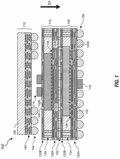
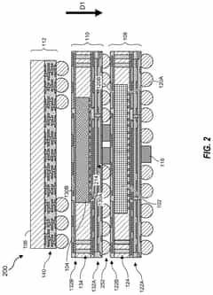
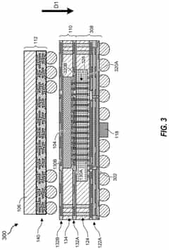
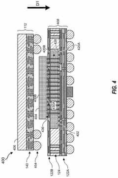
Various interconnect technologies are employed to facilitate communication between chiplets in multi-die packages. These include advanced packaging techniques such as silicon interposers, bridge chips, and through-silicon vias (TSVs) that enable high-bandwidth, low-latency connections between chiplets. These interconnect solutions address challenges related to signal integrity, power delivery, and thermal management while supporting high-speed data transfer between integrated chiplets.- Advanced Packaging Technologies for Chiplet Integration: Various packaging technologies are employed for chiplet integration, including 2.5D and 3D integration approaches. These technologies enable the connection of multiple chiplets on a common substrate or interposer, allowing for high-bandwidth, low-latency communication between different functional blocks. Advanced packaging solutions address thermal management challenges and provide improved electrical performance while enabling heterogeneous integration of chiplets manufactured using different process technologies.
- Interconnect Architectures for Chiplet-based Systems: Specialized interconnect architectures facilitate communication between chiplets in multi-die systems. These include silicon interposers, organic substrates, and advanced bridge technologies that provide high-density connections. The interconnect solutions incorporate high-speed data transfer protocols, power delivery networks, and signal integrity optimization to ensure reliable operation across chiplet boundaries while minimizing latency and power consumption.
- Design and Verification Methodologies for Chiplet Systems: Specialized design and verification methodologies address the unique challenges of chiplet-based systems. These include partitioning strategies for dividing functionality across multiple dies, interface standardization approaches, and comprehensive testing frameworks. Design tools support co-optimization of chiplets with consideration for thermal, electrical, and mechanical constraints, while verification methodologies ensure proper functionality across chiplet boundaries and under various operating conditions.
- Thermal Management Solutions for Chiplet Integration: Thermal management solutions address the heat dissipation challenges in densely packed chiplet systems. These include advanced thermal interface materials, integrated cooling structures, and thermal-aware design methodologies. The solutions optimize heat spreading across chiplets with different power densities and incorporate sensors and control systems for dynamic thermal management, ensuring reliable operation while maximizing performance within thermal constraints.
- Manufacturing and Testing Processes for Chiplet-based Systems: Specialized manufacturing and testing processes enable the production of reliable chiplet-based systems. These include advanced die-to-die bonding techniques, known-good-die testing methodologies, and yield enhancement strategies. The processes incorporate precision alignment technologies for chiplet placement, innovative approaches for handling different die thicknesses, and comprehensive test methodologies that verify both individual chiplet functionality and system-level integration.
02 Heterogeneous integration of chiplets
Heterogeneous integration involves combining chiplets manufactured using different process technologies or from different vendors into a single package. This approach allows for optimizing each component for its specific function while maintaining system-level performance. It enables the integration of logic, memory, analog, and RF components fabricated at different technology nodes, providing flexibility in design and manufacturing while potentially reducing costs and improving overall system performance.Expand Specific Solutions03 Thermal management solutions for chiplet designs
Thermal management is critical in chiplet-based designs due to high power densities and potential hotspots at interconnect points. Solutions include advanced cooling techniques, thermal interface materials, and intelligent power management systems that dynamically adjust performance based on thermal conditions. These approaches help maintain optimal operating temperatures across multiple chiplets, ensuring reliability and consistent performance while extending the lifespan of the integrated components.Expand Specific Solutions04 Testing and yield improvement for chiplet-based systems
Testing methodologies for chiplet-based systems involve pre-integration testing of individual chiplets and post-integration validation of the complete system. Known-good-die testing, built-in self-test capabilities, and advanced fault isolation techniques help identify defects early in the manufacturing process. These approaches improve overall yield by allowing manufacturers to discard only defective chiplets rather than entire monolithic dies, resulting in cost savings and more efficient use of silicon.Expand Specific Solutions05 Design automation and standardization for chiplet ecosystems
Design automation tools and standardization efforts are essential for the widespread adoption of chiplet technology. These include specialized EDA tools for multi-die design, verification, and analysis, as well as industry standards for chiplet interfaces and protocols. Standardization enables interoperability between chiplets from different vendors, while design automation tools help manage the complexity of integrating multiple dies into a cohesive system, accelerating development cycles and reducing time-to-market.Expand Specific Solutions
Leading Semiconductor Companies in Chiplet Ecosystem
Chiplet integration is transforming the semiconductor industry, currently in a growth phase characterized by rapid technological adoption and market expansion. The global chiplet market is experiencing significant momentum, projected to reach substantial scale as major players embrace this modular approach to overcome traditional monolithic design limitations. Technology maturity varies across the ecosystem, with industry leaders like TSMC, Intel, and AMD at the forefront of commercial implementation. Applied Materials and IBM are advancing manufacturing processes, while newer entrants like Chipletz are developing specialized solutions. Academic institutions including Xiduan University and Fudan University are contributing fundamental research. The industry is witnessing increased standardization efforts and ecosystem development as chiplet technology becomes essential for next-generation computing architectures, particularly for AI, high-performance computing, and data center applications.
Taiwan Semiconductor Manufacturing Co., Ltd.
Technical Solution: TSMC has pioneered advanced chiplet integration through their CoWoS (Chip-on-Wafer-on-Substrate) and InFO (Integrated Fan-Out) packaging technologies. Their CoWoS platform enables the integration of multiple silicon dies on a silicon interposer with through-silicon vias (TSVs), facilitating high-bandwidth, low-latency connections between chiplets. TSMC has continuously evolved this technology, with their latest CoWoS-S offering supporting up to 12 high-bandwidth memory (HBM) stacks and larger reticle-sized system-on-chip integration[1]. Their 3DFabric advanced packaging platform combines frontend and backend innovations to enable chiplet-based designs with enhanced performance and power efficiency. TSMC has also developed System-on-Integrated-Chips (SoIC) technology, which achieves micron-level bonding pitches for ultra-high-density interconnects between chiplets, enabling nearly monolithic-like performance in multi-die packages[2].
Strengths: Industry-leading process nodes that complement their advanced packaging; established ecosystem with major clients like AMD, Apple, and NVIDIA; proven high-volume manufacturing capability for chiplet designs. Weaknesses: High capital requirements for continued technology advancement; increasing competition from Intel and Samsung in advanced packaging; potential geopolitical vulnerabilities due to concentration of advanced packaging capabilities.
Applied Materials, Inc.
Technical Solution: Applied Materials has developed a comprehensive suite of equipment and process technologies specifically designed for chiplet integration and advanced packaging. Their Endura platform provides PVD (Physical Vapor Deposition) solutions for RDL (Redistribution Layer) metallization and barrier/seed deposition critical for chiplet interconnects. The company's Producer platform offers CVD (Chemical Vapor Deposition) and ALD (Atomic Layer Deposition) capabilities for dielectric deposition between chiplet layers. Applied Materials has also introduced the Apreo eFill system, which enables void-free copper plating for high-aspect-ratio through-silicon vias (TSVs) and hybrid bonding applications essential for vertical chiplet stacking[7]. Their Sym3 etch system provides precise via formation capabilities, while the Vistara platform offers wafer-level packaging inspection and metrology. Beyond equipment, Applied Materials has established the Advanced Packaging Development Center (APDC) in Singapore, which serves as a collaborative innovation hub where customers can develop and optimize chiplet integration processes using Applied's comprehensive toolset[8].
Strengths: Broad portfolio covering multiple critical process steps in chiplet integration; established relationships with all major semiconductor manufacturers; ability to provide end-to-end solutions for advanced packaging. Weaknesses: Dependent on overall industry adoption rates of chiplet architectures; faces competition from specialized packaging equipment providers; requires continuous high R&D investment to maintain technological leadership in rapidly evolving packaging technologies.
Key Patents and Standards in Chiplet Integration
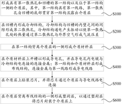
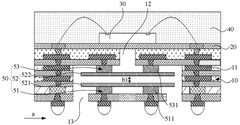
Semiconductor packaging structure and preparation method thereof
PatentActiveCN118431177B
Innovation
- A semiconductor packaging structure is designed, including a wiring structure with conductive lines, a dielectric layer, a chip and a cooling structure. The cooling structure is electrically connected to the conductive lines. After being energized, it vibrates to form an airflow pressure difference and communicates with the outside air through the first heat dissipation hole. An airflow pressure difference is formed to improve heat dissipation performance, and the chip is packaged through the dielectric layer and plastic sealing layer to avoid external power supply interference.
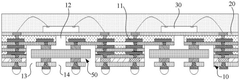
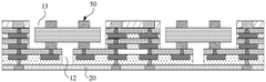
3D chiplet integration using fan-out wafer-level packaging
PatentPendingUS20240274587A1
Innovation
- The use of fan-out wafer-level packaging and three-dimensional packaging techniques for combining semiconductor chips and embedded memory in configurations such as face-to-back, back-to-back, and face-to-face orientations, enabling direct connections between chiplets and reducing assembly package sizes and manufacturing complexity.
Supply Chain Implications of Chiplet Adoption
The adoption of chiplet technology is fundamentally restructuring semiconductor supply chains, creating both opportunities and challenges across the industry. Traditional monolithic chip manufacturing relied on vertically integrated supply chains where a single company controlled most aspects of production. Chiplet architecture, however, enables a more modular and distributed approach, allowing specialized suppliers to focus on specific components that can be integrated later through advanced packaging technologies.
This shift is creating new specialized segments within the supply chain. Companies can now focus exclusively on developing specific types of chiplets—memory, processing, I/O, or analog components—rather than attempting to master all aspects of chip design and manufacturing. This specialization is enabling smaller players to enter the market and compete in specific niches, potentially democratizing parts of the semiconductor industry previously dominated by giants.
Advanced packaging technologies have become a critical link in the chiplet supply chain. As integration moves from silicon to package level, companies specializing in advanced packaging techniques like 2.5D and 3D integration are gaining strategic importance. This has elevated packaging from a relatively commoditized service to a high-value, technology-differentiated segment of the supply chain.
Standardization efforts are emerging as crucial enablers for chiplet ecosystem development. Initiatives like Universal Chiplet Interconnect Express (UCIe) are attempting to establish common interfaces and protocols that would allow chiplets from different vendors to work together seamlessly. The success of these standardization efforts will determine whether the industry evolves toward an open ecosystem with interchangeable components or remains fragmented into proprietary solutions.
Geopolitical considerations are increasingly influencing chiplet supply chain development. As nations recognize semiconductors as strategic assets, government policies are shaping where and how chiplet technologies are developed. This includes substantial investments in domestic semiconductor capabilities and restrictions on technology transfers, potentially leading to regionalized chiplet supply chains aligned with geopolitical blocs.
Inventory management and logistics are becoming more complex with chiplet adoption. Companies must coordinate the production, testing, and assembly of multiple chiplets from different suppliers, potentially located in different regions. This requires more sophisticated supply chain management systems and closer collaboration between partners, increasing the importance of digital supply chain tools and transparent information sharing.
Environmental Impact of Chiplet Manufacturing
The shift toward chiplet architecture represents a significant evolution in semiconductor manufacturing with notable environmental implications. Traditional monolithic chip production generates substantial waste due to yield issues, where defects in any part of a large die render the entire chip unusable. Chiplet integration fundamentally improves yield rates by allowing manufacturers to produce smaller components separately and combine only those that pass quality control, significantly reducing silicon waste.
Energy consumption patterns in semiconductor manufacturing are being reshaped by chiplet technology. The disaggregated approach enables more efficient use of specialized process nodes, allowing manufacturers to produce only performance-critical components using advanced nodes that require energy-intensive processes. Less critical components can be manufactured using mature nodes with lower environmental footprints, optimizing the overall energy profile of chip production.
Water usage, a critical environmental concern in semiconductor manufacturing, may see optimization through chiplet approaches. By strategically allocating manufacturing processes across different facilities based on water efficiency considerations, companies can potentially reduce the overall water footprint of complex chip systems. This distributed manufacturing model creates opportunities for more sustainable resource management.
Carbon emissions associated with semiconductor production are influenced by chiplet integration in multiple ways. While the additional packaging steps required for chiplet integration may increase certain process emissions, these are potentially offset by improved manufacturing yields and more efficient use of advanced process nodes. The net environmental impact depends on specific implementation strategies and supply chain configurations.
Material diversity in chiplet manufacturing presents both challenges and opportunities for environmental sustainability. The increased use of advanced packaging materials and interconnect technologies introduces new considerations for end-of-life management and recycling. However, the modular nature of chiplets may eventually enable more targeted component replacement and upgrades rather than wholesale device replacement, potentially extending product lifecycles.
Geographical distribution of chiplet manufacturing across multiple facilities may increase transportation-related emissions in the supply chain. However, this distributed model also creates opportunities for localized optimization of environmental controls and compliance with regional environmental regulations. Companies adopting chiplet strategies must carefully consider these trade-offs when designing their manufacturing and supply chain networks to minimize overall environmental impact.
Unlock deeper insights with Patsnap Eureka Quick Research — get a full tech report to explore trends and direct your research. Try now!
Generate Your Research Report Instantly with AI Agent
Supercharge your innovation with Patsnap Eureka AI Agent Platform!