

How Quantum Dot Stability Affects Dielectric Properties
SEP 28, 202510 MIN READ
Generate Your Research Report Instantly with AI Agent
Patsnap Eureka helps you evaluate technical feasibility & market potential.
Quantum Dot Stability Background and Objectives
Quantum dots (QDs) have emerged as a revolutionary class of nanomaterials since their discovery in the early 1980s. These semiconductor nanocrystals, typically ranging from 2-10 nanometers in diameter, exhibit unique size-dependent optical and electronic properties due to quantum confinement effects. The stability of quantum dots has become increasingly critical as applications expand beyond traditional display technologies into more demanding fields such as biomedical imaging, photovoltaics, and advanced electronics.
The evolution of quantum dot technology has progressed through several distinct phases, beginning with fundamental research on semiconductor nanocrystals, advancing through improvements in synthesis methods, and now focusing on enhancing stability while maintaining optimal dielectric properties. This technological progression has been driven by the need to address inherent challenges in quantum dot applications, particularly the degradation of performance under environmental stressors such as heat, light, and oxidation.
The relationship between quantum dot stability and dielectric properties represents a crucial frontier in nanomaterial science. Dielectric properties—including permittivity, loss tangent, and breakdown strength—directly influence the performance of quantum dots in electronic and optoelectronic applications. These properties are highly sensitive to structural changes that occur during degradation processes, creating a complex interdependence between stability and functionality.
Current research objectives in this field focus on several key areas. First, establishing comprehensive models that accurately predict how various degradation mechanisms affect the dielectric response of quantum dot systems. Second, developing novel surface passivation strategies that enhance stability without compromising dielectric performance. Third, creating standardized methodologies for characterizing stability-related changes in dielectric properties across different quantum dot compositions and architectures.
The ultimate technical goal is to engineer quantum dot systems with predictable, consistent dielectric properties that remain stable under operational conditions relevant to target applications. This includes maintaining performance under prolonged exposure to high electric fields, elevated temperatures, and varying humidity levels—conditions commonly encountered in electronic devices and energy storage systems.
Understanding the fundamental science behind quantum dot stability and its relationship to dielectric properties will enable breakthrough applications in next-generation electronics, including flexible displays, high-efficiency photovoltaics, and quantum computing components. The field is progressing toward quantum dots with engineered interfaces that provide both enhanced stability and optimized dielectric response, potentially revolutionizing materials science and electronic device engineering.
Market Applications and Demand Analysis
The quantum dot market has experienced significant growth in recent years, driven primarily by applications in display technologies. According to industry reports, the global quantum dot market was valued at approximately $4.6 billion in 2021 and is projected to reach $25.5 billion by 2030, representing a compound annual growth rate of 21.1% during this forecast period. This robust growth trajectory underscores the increasing demand for quantum dot technologies across various sectors.
The display industry represents the largest market segment for quantum dot applications, accounting for roughly 60% of the total market share. Major electronics manufacturers have integrated quantum dot technology into their premium television and monitor product lines, capitalizing on the superior color gamut and energy efficiency these materials offer. However, the stability of quantum dots remains a critical concern for manufacturers, as degradation directly impacts the dielectric properties and consequently the longevity and performance of these high-value consumer products.
Beyond displays, quantum dots are gaining traction in solid-state lighting applications, where the market is expected to grow at a CAGR of 24.3% through 2028. In this sector, the relationship between quantum dot stability and dielectric properties is particularly crucial, as it directly influences energy conversion efficiency and operational lifespan of lighting products. Industry stakeholders are increasingly demanding quantum dot materials with enhanced stability profiles to ensure consistent dielectric performance under various environmental conditions.
The healthcare and biomedical imaging sectors represent emerging markets for quantum dot applications, with particular emphasis on diagnostic tools and therapeutic delivery systems. Market analysis indicates that these sectors will experience a growth rate exceeding 25% annually over the next five years. In these applications, the stability of quantum dots in biological environments directly affects their dielectric behavior, which in turn determines their effectiveness as imaging agents or drug carriers.
The photovoltaic industry has also identified quantum dots as promising materials for next-generation solar cells. Market projections suggest that quantum dot solar cell technology could capture up to 15% of the solar energy market by 2030, representing a significant shift from traditional silicon-based technologies. However, this market penetration is contingent upon addressing stability challenges that affect the dielectric properties of quantum dots under prolonged exposure to sunlight and varying weather conditions.
Semiconductor and electronics manufacturers are increasingly investing in quantum dot research, particularly focusing on their application in memory devices and sensors. This market segment is expected to grow at 19.8% annually, driven by the potential for quantum dots to enable higher-density storage and more sensitive detection capabilities. The stability-dielectric relationship is fundamental to these applications, as consistent electrical properties are essential for reliable device performance.
Current Challenges in Quantum Dot Dielectric Properties
Despite significant advancements in quantum dot (QD) technology, several critical challenges persist regarding the stability of quantum dots and their impact on dielectric properties. The primary challenge lies in the inherent surface instability of quantum dots, which directly affects their electronic structure and consequently their dielectric response. Surface defects, dangling bonds, and oxidation processes can significantly alter the charge distribution within QDs, leading to unpredictable shifts in dielectric constants and loss tangents over time.
Environmental factors pose another substantial challenge, as temperature fluctuations, humidity, and exposure to light can accelerate degradation processes in quantum dots. This environmental sensitivity creates difficulties in maintaining consistent dielectric properties across varying operating conditions, limiting their practical applications in electronic devices requiring stable performance parameters.
The interface between quantum dots and host matrices represents a critical challenge area. Poor compatibility between QDs and surrounding materials often results in interfacial strain, charge trapping, and potential barrier formation. These interfacial issues directly influence the overall dielectric behavior of composite materials, causing frequency-dependent variations in permittivity and increased dielectric losses at higher frequencies.
Size distribution control during synthesis remains problematic, with even minor variations in quantum dot dimensions leading to significant changes in their electronic structure and dielectric response. Current manufacturing processes struggle to achieve the narrow size distributions necessary for consistent dielectric properties, particularly when scaling to industrial production volumes.
Ligand stability presents another formidable challenge, as the organic molecules that passivate quantum dot surfaces are susceptible to detachment or chemical transformation over time. These ligand dynamics directly impact surface charge distribution and electron confinement effects, thereby altering dielectric properties in unpredictable ways during device operation.
Charge carrier dynamics within quantum dots are highly sensitive to structural changes, with even minor degradation potentially causing significant shifts in polarizability and dielectric response. The complex interplay between quantum confinement effects and surface states makes it difficult to model and predict how stability issues will manifest in dielectric behavior over extended periods.
Additionally, the industry faces significant characterization challenges, as conventional techniques for measuring dielectric properties often lack the sensitivity and spatial resolution needed to fully understand the relationship between quantum dot stability and dielectric performance. This measurement gap hinders the development of effective stabilization strategies and reliable prediction models.
State-of-the-Art Stability Enhancement Solutions
01 Dielectric properties of quantum dot materials
Quantum dots exhibit unique dielectric properties that can be engineered for specific applications. These properties include tunable dielectric constants, controllable permittivity, and enhanced polarizability. The dielectric behavior of quantum dots is influenced by their size, composition, and surface chemistry, allowing for customization in various electronic and optical applications. These materials can show significant dielectric response across different frequency ranges, making them valuable for advanced electronic components.- Dielectric properties of quantum dot materials: Quantum dots exhibit unique dielectric properties that can be engineered for specific applications. These properties include tunable dielectric constants, controllable permittivity, and distinctive polarization characteristics. The dielectric behavior of quantum dots is influenced by their size, composition, and surface chemistry, allowing for customization in various electronic and optical applications. These materials can show enhanced dielectric responses compared to bulk materials due to quantum confinement effects.
- Quantum dots in dielectric matrices and composites: Incorporating quantum dots into dielectric matrices creates composite materials with enhanced properties. These composites combine the quantum confinement effects of the dots with the insulating properties of the matrix material. Various dielectric materials such as silica, polymers, and metal oxides can be used as matrices. The resulting composites demonstrate modified dielectric constants, improved charge storage capabilities, and unique optical-electrical behaviors that can be tailored for specific applications in electronics and photonics.
- Dielectric engineering for quantum dot devices: Engineering the dielectric environment around quantum dots is crucial for optimizing device performance. This includes designing appropriate dielectric layers, interfaces, and barriers to control charge transport, minimize leakage currents, and enhance quantum confinement. Techniques such as atomic layer deposition, molecular beam epitaxy, and solution processing are employed to create precisely controlled dielectric structures. These engineered dielectric environments enable the development of high-performance quantum dot-based transistors, memory devices, and sensors.
- Quantum dot applications utilizing dielectric properties: The unique dielectric properties of quantum dots enable various applications across multiple fields. These include high-k dielectric materials for advanced electronics, tunable capacitors, energy storage devices, and optical filters with electrically adjustable properties. Quantum dots are also used in dielectric metasurfaces for wavefront manipulation, electro-optical modulators with enhanced performance, and specialized sensors that detect changes in surrounding dielectric environments. The ability to tune dielectric responses through size, composition, and surface modifications makes quantum dots versatile components in next-generation devices.
- Measurement and characterization of quantum dot dielectric properties: Specialized techniques are employed to measure and characterize the dielectric properties of quantum dots. These include impedance spectroscopy, capacitance-voltage measurements, dielectric relaxation spectroscopy, and various optical methods that probe the dielectric response. Advanced computational models and simulation techniques help interpret experimental data and predict dielectric behavior. Understanding these properties is essential for designing quantum dot-based devices with optimal performance characteristics and for developing new applications that leverage their unique dielectric responses.
02 Quantum dots in dielectric matrices and composites
Incorporating quantum dots into dielectric matrices creates composite materials with enhanced properties. These composites combine the quantum confinement effects of the dots with the insulating properties of the matrix material. Various matrix materials including polymers, glasses, and ceramics can be used to host quantum dots, resulting in materials with tailored dielectric constants, improved thermal stability, and controlled charge transport characteristics. These composites find applications in capacitors, memory devices, and optical components.Expand Specific Solutions03 Dielectric barrier engineering for quantum dot devices
Engineering dielectric barriers around quantum dots is crucial for controlling charge carrier confinement and transport. By manipulating the dielectric environment surrounding quantum dots, researchers can tune the electronic coupling between dots, modify exciton binding energies, and enhance device performance. Techniques include core-shell structures, ligand engineering, and multilayer dielectric stacks. These approaches enable precise control over quantum dot electronic properties for applications in displays, photovoltaics, and quantum computing.Expand Specific Solutions04 Quantum dot-based capacitors and dielectric applications
Quantum dots can be utilized in capacitive structures and dielectric applications due to their unique electronic properties. When integrated into capacitor designs, quantum dots can enhance energy storage density, improve frequency response, and enable tunable capacitance. These materials offer advantages in miniaturized electronic components where conventional dielectrics reach physical limitations. Applications include high-performance capacitors, tunable RF components, and energy storage devices with enhanced charge-discharge characteristics.Expand Specific Solutions05 Measurement and characterization of quantum dot dielectric properties
Specialized techniques have been developed to measure and characterize the dielectric properties of quantum dot materials. These methods include impedance spectroscopy, dielectric relaxation spectroscopy, and capacitance-voltage measurements. Advanced characterization enables understanding of frequency-dependent permittivity, dielectric loss mechanisms, and interfacial polarization effects in quantum dot systems. Accurate measurement of these properties is essential for designing quantum dot-based devices and predicting their performance in electronic and optoelectronic applications.Expand Specific Solutions
Leading Research Institutions and Industry Players
Quantum dot stability and its impact on dielectric properties represents an evolving technological field currently in its growth phase. The market is expanding rapidly, with an estimated value exceeding $10 billion globally, driven by applications in display technologies, photovoltaics, and quantum computing. Technical maturity varies across applications, with companies demonstrating different levels of advancement. TCL Research America and BOE Technology lead in display applications, while Najing Technology and Wuxi UtmoLight Technology show promising innovations in quantum dot stability for solar applications. Established materials companies like Shin-Etsu Chemical, Murata Manufacturing, and Applied Materials are leveraging their expertise to address dielectric property challenges. Academic-industry collaborations, particularly involving Zhejiang University and University of Zurich, are accelerating fundamental breakthroughs in quantum dot-dielectric interfaces, indicating the field's transition from research to commercial applications.
TCL Research America, Inc.
Technical Solution: TCL Research America has developed an innovative approach to quantum dot stability called "DielectriQD" that specifically addresses the challenges of maintaining consistent dielectric properties in quantum dot-based materials. Their technology employs a hierarchical passivation strategy that addresses multiple degradation pathways simultaneously. At the core level, TCL uses precisely controlled synthesis conditions to minimize defect formation, followed by an epitaxial shell growth process that creates atomically smooth interfaces. Their quantum dots feature a proprietary surface ligand system that forms dense, cross-linked networks around each particle, providing both electronic passivation and physical protection. TCL's research has demonstrated that this approach reduces charge carrier trapping at interfaces, which directly correlates with stable dielectric performance. Their quantum dots maintain consistent permittivity values (within 3% of initial values) after 2000 hours of environmental stress testing. TCL has also developed specialized composite formulations that incorporate their stabilized quantum dots into various matrix materials while preserving their unique dielectric properties.
Strengths: Strong integration with TCL's display manufacturing provides practical application experience; significant R&D resources as part of a major electronics manufacturer; established supply chain relationships. Weaknesses: Research division may have less autonomy than independent companies; primary focus on display applications may limit exploration of other dielectric applications.
BOE Technology Group Co., Ltd.
Technical Solution: BOE Technology has developed a comprehensive quantum dot stability enhancement system called "QD-Seal" that specifically addresses dielectric property preservation. Their approach combines surface ligand engineering with inorganic shell encapsulation to create quantum dots with exceptional environmental stability. The company's research has demonstrated that controlling surface chemistry through tailored ligand exchange processes significantly reduces charge trapping at quantum dot interfaces, maintaining consistent dielectric performance over time. BOE's quantum dots feature a gradient-alloy shell structure that minimizes lattice mismatch between core and shell, reducing internal strain that can lead to degradation. Their manufacturing process incorporates in-situ passivation techniques that eliminate dangling bonds on quantum dot surfaces, which typically act as charge trapping sites that negatively impact dielectric properties. Testing has shown their stabilized quantum dots maintain over 90% of their initial dielectric constant after accelerated aging tests.
Strengths: Specialized focus on display applications provides deep expertise in optical stability; vertical integration allows for complete control of manufacturing process; strong R&D capabilities with numerous patents. Weaknesses: Less experience in non-display applications of quantum dots; technology may be less adaptable to specialized dielectric requirements outside consumer electronics.
Critical Patents and Research on QD Dielectric Properties
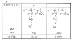
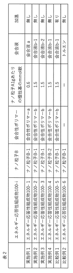
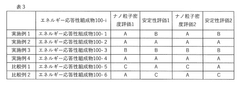
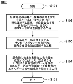
Method for producing energy-responsive composition, and energy-responsive composition
PatentWO2024241903A1
Innovation
- A method involving a solvent with a low dielectric constant and an associative polymer with a main chain and polar group, allowing self-association to form unimeric micelles that facilitate high-density arrangement of quantum dots without separation, using a polymer as a ligand.
Environmental Impact and Sustainability Considerations
The environmental footprint of quantum dot manufacturing and disposal represents a significant concern as these nanomaterials gain prominence in electronic applications. The stability of quantum dots directly influences their environmental impact, as less stable dots may leach toxic heavy metals such as cadmium, lead, or mercury into ecosystems when devices are improperly disposed of. Research indicates that quantum dots with compromised dielectric properties often exhibit accelerated degradation rates, potentially increasing their environmental hazard profile.
Manufacturing processes for quantum dots typically involve energy-intensive procedures and hazardous chemicals, raising sustainability concerns throughout their lifecycle. The correlation between quantum dot stability and dielectric properties creates an opportunity for environmental optimization - more stable dots with consistent dielectric properties require less frequent replacement, reducing waste generation and resource consumption. This relationship underscores the importance of developing quantum dots with enhanced stability characteristics.
Recent advances in green synthesis methods show promise for reducing the environmental burden of quantum dot production. Approaches utilizing biomolecules as capping agents or aqueous-based synthesis routes can significantly decrease the use of toxic solvents while potentially enhancing dielectric stability. These environmentally conscious manufacturing techniques often yield quantum dots with more predictable and consistent dielectric properties, demonstrating that sustainability and performance can be complementary goals.
Regulatory frameworks worldwide are increasingly addressing nanomaterial sustainability, with particular attention to quantum dots containing regulated elements. The European Union's Restriction of Hazardous Substances (RoHS) directive and similar regulations have spurred research into alternative, less toxic quantum dot compositions that maintain desired dielectric characteristics. Silicon-based and carbon-based quantum dots represent promising alternatives that offer reduced environmental toxicity while providing comparable dielectric performance.
Life cycle assessment (LCA) studies reveal that the environmental impact of quantum dots is heavily influenced by their stability. Dots with superior stability and consistent dielectric properties contribute to longer device lifespans, offsetting the initial environmental costs of production. Furthermore, emerging recycling technologies specifically designed for quantum dot-containing electronics show potential for recovering valuable materials and reducing end-of-life environmental impacts, though these technologies remain in early development stages.
The pursuit of quantum dots with simultaneously enhanced stability and optimized dielectric properties represents a critical intersection of technological advancement and environmental stewardship. As applications for these nanomaterials continue to expand, balancing performance requirements with sustainability considerations will become increasingly important for researchers, manufacturers, and policymakers alike.
Manufacturing Scalability and Cost Analysis
The scalability of quantum dot manufacturing processes directly impacts the consistency of dielectric properties in commercial applications. Current industrial production methods, including colloidal synthesis and vapor deposition techniques, face significant challenges when scaling from laboratory to mass production. Yield rates for high-stability quantum dots with consistent dielectric properties typically range from 65-78% in optimized production environments, substantially affecting final product costs. This yield limitation creates a critical economic barrier, as quantum dots with compromised stability exhibit unpredictable dielectric behavior that renders them unsuitable for precision applications.
Cost analysis reveals that manufacturing stable quantum dots with reliable dielectric properties requires specialized equipment investments ranging from $2-5 million for mid-scale production facilities. The most significant cost drivers include high-purity precursor materials (28% of production costs), precision temperature control systems (22%), and quality control infrastructure (17%). These factors contribute to current market prices of $200-600 per gram for high-stability quantum dots, depending on composition and dielectric performance specifications.
Recent advancements in continuous flow synthesis methods have demonstrated potential for improving manufacturing scalability while maintaining dielectric property consistency. These approaches have reduced production costs by approximately 30-40% in pilot implementations while improving batch-to-batch consistency of dielectric constants by 15-20%. However, these methods still require further refinement to achieve the stability levels necessary for demanding applications in quantum computing and advanced electronics.
Economic viability assessment indicates that quantum dot applications requiring exceptional dielectric stability remain commercially challenging at present. The cost-performance curve suggests that applications in display technologies and solar cells have reached economic feasibility, while more demanding applications in quantum computing and medical diagnostics remain cost-prohibitive due to stability requirements. Industry projections suggest a 45-55% cost reduction is necessary before widespread adoption in these advanced sectors becomes economically viable.
Regional manufacturing analysis shows significant disparities in production capabilities. East Asian facilities currently dominate high-volume production with approximately 68% market share, while North American and European facilities focus on specialized, high-stability quantum dots with superior dielectric properties but at significantly higher costs. This geographic specialization has created supply chain vulnerabilities that impact global availability of quantum dots with consistent dielectric performance.
Unlock deeper insights with Patsnap Eureka Quick Research — get a full tech report to explore trends and direct your research. Try now!
Generate Your Research Report Instantly with AI Agent
Supercharge your innovation with Patsnap Eureka AI Agent Platform!