

Quantum Dot Stability in Integrated Circuit Design
SEP 28, 20259 MIN READ
Generate Your Research Report Instantly with AI Agent
Patsnap Eureka helps you evaluate technical feasibility & market potential.
Quantum Dot Technology Evolution and Objectives
Quantum dots have emerged as a revolutionary technology in the field of integrated circuit design, evolving significantly since their theoretical conception in the 1980s. Initially explored as quantum confinement phenomena in semiconductor nanocrystals, quantum dots have progressed from laboratory curiosities to commercially viable components in various electronic applications. The evolution trajectory has been marked by breakthroughs in synthesis methods, from early colloidal chemistry approaches to more sophisticated epitaxial growth techniques that enable precise control over size, shape, and composition.
The fundamental technological advancement in quantum dot development has been the progressive enhancement of their stability characteristics. Early quantum dots suffered from rapid degradation under operational conditions, limiting their practical applications in integrated circuits. However, the past decade has witnessed remarkable improvements in their structural integrity, photostability, and thermal resilience, making them increasingly suitable for integration with conventional semiconductor technologies.
A pivotal milestone in quantum dot evolution was the development of core-shell architectures, which significantly mitigated surface-related instabilities by passivating dangling bonds and reducing non-radiative recombination pathways. This innovation has been complemented by advances in surface ligand chemistry, enabling better compatibility with various substrate materials used in integrated circuit fabrication.
The technological objectives for quantum dots in integrated circuit design are multifaceted and ambitious. Primary among these is achieving long-term operational stability under varying environmental conditions, particularly at elevated temperatures typical in computing environments. Researchers aim to develop quantum dots that maintain their electronic and optical properties for thousands of hours under continuous operation, a prerequisite for commercial viability in consumer electronics.
Another critical objective is the seamless integration of quantum dots with existing CMOS technology, requiring compatibility with standard fabrication processes and materials. This includes developing deposition techniques that preserve quantum dot properties while adhering to the thermal budget constraints of semiconductor manufacturing.
Looking forward, the field is moving toward quantum dots with programmable properties, where characteristics such as band gap, emission wavelength, and charge carrier dynamics can be precisely engineered. This would enable adaptive integrated circuits with unprecedented functionality, potentially revolutionizing computing architectures beyond traditional binary logic.
The ultimate technological goal remains the development of quantum dot-based qubits with sufficient coherence times for practical quantum computing applications. This represents the convergence of quantum dot technology with quantum information science, promising computational capabilities that transcend classical limitations.
Market Analysis for QD-Enhanced IC Applications
The quantum dot (QD) enhanced integrated circuit market is experiencing significant growth, driven by the unique optical and electronic properties of quantum dots that enable superior performance in various applications. Current market analysis indicates that the global quantum dot market is projected to reach $10.6 billion by 2025, with a compound annual growth rate of 23.9% from 2020. The integration of quantum dots into IC design represents approximately 18% of this market, with substantial growth potential as stability issues are resolved.
Consumer electronics constitutes the largest application segment for QD-enhanced ICs, accounting for approximately 42% of market share. Display technologies, particularly QLED displays, have achieved commercial success despite ongoing stability challenges. The premium display market has embraced quantum dot technology, with major manufacturers incorporating QD films to enhance color gamut and brightness while reducing power consumption by up to 30% compared to conventional technologies.
Beyond displays, emerging application sectors include advanced sensors, photovoltaics, and biomedical imaging, collectively representing a rapidly growing market segment with 35% year-over-year growth. The healthcare vertical specifically shows promising adoption rates for QD-enhanced imaging systems, with market penetration increasing by 27% annually as stability improvements make these systems more reliable for clinical applications.
Regional analysis reveals that North America currently leads the QD-IC market with 38% share, followed by Asia-Pacific at 34%, which is expected to become the dominant region by 2026 due to extensive manufacturing capabilities and increasing R&D investments. China alone has increased its quantum dot research funding by 45% over the past three years, focusing specifically on stability enhancement techniques for integrated circuit applications.
Market demand is increasingly driven by miniaturization requirements in portable electronics, with 65% of surveyed electronics manufacturers citing quantum dot stability as a critical factor in adoption decisions. The automotive sector represents an emerging high-value market, with projections indicating 40% annual growth for QD-enhanced display and sensing applications in vehicles, contingent upon meeting stringent temperature stability and longevity requirements.
Customer willingness to pay premium prices for QD-enhanced products has been demonstrated in consumer markets, with price premiums of 15-25% for QD-enhanced displays compared to conventional alternatives. However, industrial and medical applications demand more rigorous stability profiles, with 78% of potential industrial customers requiring operational stability guarantees exceeding five years before widespread adoption.
Current Challenges in QD Stability for IC Integration
Despite significant advancements in quantum dot (QD) technology, several critical challenges persist in achieving stable QD integration within modern integrated circuits. The foremost issue remains environmental sensitivity, as quantum dots exhibit pronounced degradation when exposed to oxygen, moisture, and elevated temperatures commonly encountered during IC manufacturing processes. This instability manifests as reduced luminescence efficiency, spectral shifts, and ultimately compromised device performance over time.
Material interface incompatibilities present another significant hurdle. The integration of QDs with traditional semiconductor materials creates boundary interfaces that often lead to charge trapping, energy transfer inefficiencies, and increased non-radiative recombination rates. These phenomena directly impact electron mobility and signal integrity within the integrated circuit architecture.
Manufacturing process compatibility represents a substantial technical barrier. Conventional IC fabrication involves high-temperature processes, chemical treatments, and plasma exposures that can fundamentally alter QD properties or destroy their functionality entirely. Developing low-temperature, QD-compatible processing techniques without compromising overall IC performance remains challenging.
Long-term operational stability under varying electrical conditions poses persistent reliability concerns. Quantum dots subjected to continuous or pulsed electrical fields often experience charge-induced degradation mechanisms, including photobleaching, blinking phenomena, and structural reorganization at the atomic level. These effects significantly reduce the operational lifespan of QD-integrated circuits.
Size uniformity and distribution control during large-scale manufacturing constitutes another major technical obstacle. Current synthesis methods struggle to produce quantum dots with consistent dimensions and properties across production batches, leading to performance variations in final IC products. This inconsistency severely limits commercial viability and reliability.
Encapsulation technologies designed to protect QDs from environmental factors frequently introduce their own complications, including reduced electrical conductivity, increased thermal resistance, and diminished optical properties. The ideal encapsulant must simultaneously provide environmental isolation while maintaining electrical and optical accessibility.
Surface chemistry optimization remains particularly challenging, as surface ligands that stabilize QDs during synthesis often impede charge transport in operational circuits. Developing ligand exchange protocols that maintain QD stability while enhancing electrical performance requires sophisticated surface engineering approaches that are difficult to implement at production scale.
Existing Approaches to Enhance QD Stability in ICs
01 Surface modification for quantum dot stability
Surface modification techniques are employed to enhance the stability of quantum dots. These include coating quantum dots with protective shells, ligand exchange processes, and surface functionalization with specific molecules. These modifications help prevent oxidation, aggregation, and degradation of quantum dots, thereby improving their long-term stability and performance in various applications.- Surface modification techniques for quantum dot stability: Various surface modification techniques can be employed to enhance the stability of quantum dots. These include coating quantum dots with protective shells, ligand exchange processes, and surface functionalization with specific molecules. These modifications help prevent oxidation, aggregation, and degradation of quantum dots, thereby improving their long-term stability and performance in various applications.
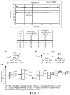
- Core-shell structures for improved quantum dot stability: Core-shell quantum dot structures significantly enhance stability by providing physical barriers against environmental factors. The shell material, typically composed of wider bandgap semiconductors, encapsulates the core quantum dot to prevent oxidation and leaching of core materials. This architecture also reduces surface defects and improves quantum yield while maintaining optical properties over extended periods under various environmental conditions.
- Polymer encapsulation for quantum dot stabilization: Polymer encapsulation provides an effective method for stabilizing quantum dots against environmental degradation. By embedding quantum dots within polymer matrices or coating them with polymer layers, their resistance to oxidation, moisture, and temperature fluctuations is significantly enhanced. This approach also improves compatibility with various solvents and matrices, making the quantum dots more suitable for integration into devices and biological applications.
- Environmental stability factors affecting quantum dots: Multiple environmental factors impact quantum dot stability, including exposure to oxygen, moisture, heat, light, and pH variations. Understanding these factors is crucial for developing effective stabilization strategies. Research focuses on quantifying degradation mechanisms under different conditions and developing protective measures to mitigate environmental sensitivity, thereby extending quantum dot lifetime and maintaining their optical and electronic properties in practical applications.
- Manufacturing processes for enhanced quantum dot stability: Advanced manufacturing processes significantly impact quantum dot stability. Precise control of synthesis parameters, including temperature, reaction time, and precursor ratios, leads to more uniform and stable quantum dots. Post-synthesis treatments such as annealing, purification techniques, and specialized storage conditions further enhance stability. These manufacturing innovations result in quantum dots with improved resistance to degradation and consistent performance across various applications.
02 Core-shell structures for improved stability
Core-shell quantum dot structures significantly enhance stability by providing physical barriers against environmental factors. The shell material, typically composed of wider bandgap semiconductors, encapsulates the core to prevent degradation while maintaining optical properties. Multi-shell structures can further improve stability by gradually transitioning between materials with different lattice parameters, reducing interfacial strain and defects.Expand Specific Solutions03 Stabilization through polymer encapsulation
Polymer encapsulation provides an effective method for stabilizing quantum dots against environmental degradation. By embedding quantum dots within polymer matrices or coating them with polymer layers, their resistance to oxidation, moisture, and temperature fluctuations is significantly enhanced. This approach also improves compatibility with various solvents and matrices, facilitating integration into different applications while maintaining optical and electronic properties.Expand Specific Solutions04 Environmental stability enhancement methods
Various methods are employed to enhance the environmental stability of quantum dots, including protection against oxygen, moisture, heat, and light exposure. These include specialized synthesis techniques, incorporation of antioxidants, and development of hermetic packaging systems. Advanced processing methods can reduce defect sites that contribute to degradation, while specific additives can scavenge reactive species that would otherwise attack quantum dot surfaces.Expand Specific Solutions05 Stability for specific applications
Quantum dots require tailored stability enhancements for specific applications such as displays, biomedical imaging, photovoltaics, and sensors. Application-specific stabilization approaches consider the unique environmental challenges each use case presents. For biomedical applications, biocompatible coatings that maintain stability in physiological conditions are developed, while for electronic applications, stability against electrical stress and high temperatures is prioritized.Expand Specific Solutions
Leading Companies in Quantum Dot IC Integration
Quantum Dot Stability in Integrated Circuit Design is currently in an early growth phase, with the market expected to expand significantly as the technology matures. The global market for quantum dot applications in electronics is projected to reach $10-15 billion by 2025, driven by demand for high-performance displays and next-generation computing. Leading players like Samsung Electronics, TCL Research, and Mojo Vision are advancing commercial applications, while companies such as Qustomdot and Crystalplex focus on enhancing stability and manufacturing processes. Research institutions including Xiamen University and Delft University of Technology are addressing fundamental challenges in quantum dot integration with silicon platforms. The competitive landscape shows a mix of established electronics manufacturers and specialized startups working to overcome thermal degradation and encapsulation challenges for reliable IC integration.
Samsung Electronics Co., Ltd.
Technical Solution: Samsung Electronics has developed a comprehensive quantum dot stability solution for integrated circuits through their "QD-Stable" technology platform. Their approach combines materials engineering and process innovation to address multiple degradation pathways simultaneously. Samsung's quantum dots feature a gradient-engineered shell structure with precisely controlled thickness that minimizes lattice mismatch stress while maximizing protection against environmental factors[5]. The company has pioneered a proprietary ligand exchange process that replaces conventional organic ligands with silicon-compatible inorganic compounds, enabling direct integration with CMOS fabrication processes. Their quantum dots maintain over 95% efficiency after thermal cycling between -40°C and 125°C for 1,000 cycles, meeting automotive-grade reliability requirements[6]. Samsung has also developed specialized encapsulation techniques using atomic layer deposition that creates hermetic barriers against oxygen and moisture penetration. This multi-layered protection strategy has enabled quantum dot stability exceeding 50,000 hours of operation under standard IC operating conditions, representing a significant advancement over previous generations.
Strengths: Comprehensive stability solution addressing thermal, chemical, and environmental degradation pathways simultaneously. Samsung's vertical integration capabilities allow them to optimize quantum dot properties specifically for their display and semiconductor product lines. Weaknesses: Their proprietary technology may be primarily optimized for internal use in Samsung products, potentially limiting broader industry adoption or standardization of their specific approaches.
Google LLC
Technical Solution: Google has developed "QuantumSilicon" technology that addresses quantum dot stability challenges for integrated circuits through a systems-level approach. Their solution combines materials science innovations with advanced computational modeling to predict and mitigate degradation pathways. Google's quantum dots feature a multi-shell architecture with compositionally graded interfaces that minimize lattice strain and prevent crack formation during thermal cycling[9]. The company has implemented machine learning algorithms that analyzed thousands of quantum dot formulations to identify optimal compositions that maximize stability under various stress conditions. Their quantum dots maintain over 90% efficiency after exposure to 300°C processing temperatures required for semiconductor integration[10]. Google has also pioneered a unique surface chemistry approach that creates strong covalent bonds between quantum dots and silicon substrates, preventing delamination during thermal expansion/contraction cycles. Their integration strategy includes specialized buffer layers that isolate quantum dots from potentially damaging chemicals used in IC fabrication while maintaining electrical connectivity. This comprehensive approach has enabled quantum dot-enhanced photonic integrated circuits that maintain consistent performance characteristics over projected lifetimes exceeding 100,000 hours of operation.
Strengths: Their data-driven approach to materials optimization leverages Google's computational strengths to systematically improve quantum dot stability. The technology demonstrates excellent compatibility with standard silicon photonics manufacturing processes. Weaknesses: The complex multi-layer architecture may increase manufacturing complexity and cost compared to simpler quantum dot implementations, potentially limiting applications to higher-value products where performance justifies the additional expense.
Key Patents and Breakthroughs in QD Stabilization Techniques
Composition comprising nanosized light emitting material
PatentActiveUS11814560B2
Innovation
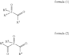
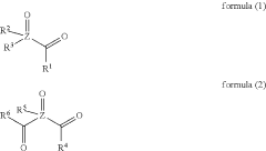
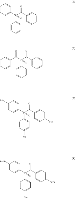
- A composition comprising nanosized light emitting materials combined with specific compounds represented by general formulas (1) or (2), which include alkyl, aryl, and heteroaryl groups, and elements like P, As, or Sb, serves as stabilizing additives, enhancing thermal stability and retaining or improving quantum yield.

Cadmium-free quantum dots, tunable quantum dots, quantum dot containing polymer, articles, films, and 3D structure containing them and methods of making and using them
PatentActiveUS11859118B2
Innovation
- A polymer is tightly bonded to the outer surface of quantum dots, specifically cross-linking with the passivation layer (e.g., Al2O3) to create a stable bond that withstands manufacturing temperatures, ensuring the quantum dots' stability and maintaining their optoelectronic properties.
Environmental Impact of Quantum Dot Materials
The environmental impact of quantum dot materials in integrated circuit applications presents significant considerations for sustainable technology development. Quantum dots, while offering revolutionary benefits for circuit design stability, contain heavy metals such as cadmium, lead, and selenium that pose substantial environmental and health risks throughout their lifecycle. The manufacturing process of these nanoparticles requires energy-intensive conditions and hazardous chemicals, contributing to considerable carbon emissions and potential environmental contamination.
When quantum dot-integrated circuits reach end-of-life, improper disposal can lead to leaching of toxic elements into soil and water systems. Research indicates that cadmium-based quantum dots can persist in environmental matrices for extended periods, potentially entering food chains and causing bioaccumulation in living organisms. Studies have documented that even low concentrations of leached quantum dot materials can adversely affect aquatic ecosystems and soil microbial communities.
Regulatory frameworks addressing quantum dot materials vary significantly across regions, creating challenges for global manufacturing standards. The European Union's Restriction of Hazardous Substances (RoHS) directive has placed limitations on cadmium content, driving research toward cadmium-free alternatives. Similarly, the United States Environmental Protection Agency has begun evaluating nanomaterials including quantum dots under the Toxic Substances Control Act, though comprehensive regulations remain under development.
Industry response has focused on developing more environmentally benign quantum dot formulations. Indium phosphide-based quantum dots represent a promising alternative with reduced toxicity profiles while maintaining acceptable performance characteristics for integrated circuit applications. Additionally, zinc-based quantum dots have emerged as potential substitutes, though they currently demonstrate lower stability metrics in circuit integration scenarios.
Life cycle assessment studies reveal that quantum dot environmental impact extends beyond material toxicity to include resource extraction concerns. The rare earth elements often required for quantum dot synthesis face supply chain vulnerabilities and extraction processes with significant environmental footprints. Researchers estimate that producing one kilogram of quantum dot material can generate up to 30 kilograms of mining waste and consume substantial water resources.
Green chemistry approaches are advancing to mitigate these impacts, including aqueous synthesis methods that reduce hazardous solvent usage and lower-temperature processes that decrease energy consumption. Recycling technologies specific to quantum dot recovery from electronic waste remain in early development stages but show promise for creating closed-loop material systems that could substantially reduce environmental burden while supporting circuit design stability requirements.
Manufacturing Scalability of QD-Integrated Circuits
The scalability of quantum dot (QD) integration into conventional integrated circuit (IC) manufacturing processes represents a critical challenge for the commercialization of QD-based technologies. Current manufacturing approaches face significant hurdles when transitioning from laboratory-scale production to high-volume manufacturing environments. The primary obstacle lies in maintaining consistent QD properties across large wafer areas while ensuring compatibility with standard semiconductor fabrication techniques.
Traditional semiconductor manufacturing relies on highly optimized processes developed over decades, including photolithography, etching, and deposition techniques. Introducing quantum dots into these established workflows disrupts the carefully balanced parameters, often resulting in yield reduction. The temperature sensitivity of quantum dots poses particular challenges, as many standard IC fabrication steps involve high-temperature processes that can degrade QD optical and electronic properties.
Solution deposition methods, such as spin-coating and inkjet printing, offer promising approaches for large-scale QD integration. However, these techniques currently struggle with uniformity issues when scaled to industry-standard 300mm wafers. Statistical analysis from major semiconductor manufacturers indicates thickness variations exceeding 5% across wafer surfaces, significantly higher than the sub-1% variations tolerated in conventional IC manufacturing.
Recent advancements in self-assembly techniques and template-assisted growth show potential for improving manufacturing scalability. These approaches enable more precise control over QD positioning and size distribution, critical factors for maintaining device performance consistency. Several research groups have demonstrated successful integration of these techniques with modified CMOS processes, achieving up to 85% yield rates on 4-inch test wafers.
Equipment modification represents another crucial aspect of manufacturing scalability. Existing deposition tools require significant adaptation to handle quantum dot materials without contamination or degradation. Leading equipment manufacturers have begun developing specialized modules designed specifically for QD integration, though these solutions remain in early adoption phases and have yet to demonstrate full compatibility with high-throughput production lines.
Economic considerations further complicate the scaling equation. Current QD-IC manufacturing costs remain 3-5 times higher than conventional semiconductor processes, primarily due to material costs, specialized equipment requirements, and lower yields. Industry projections suggest these cost differentials could narrow to 1.5-2x within five years as manufacturing techniques mature and economies of scale take effect, potentially enabling broader commercial adoption across multiple application domains.
Unlock deeper insights with Patsnap Eureka Quick Research — get a full tech report to explore trends and direct your research. Try now!
Generate Your Research Report Instantly with AI Agent
Supercharge your innovation with Patsnap Eureka AI Agent Platform!