How To Maximize Conductive Properties Of Tungsten?
Tungsten Conductivity Enhancement Objectives
Tungsten, renowned for its exceptional thermal and electrical conductivity, has long been a material of interest in various high-performance applications. The objective of maximizing the conductive properties of tungsten is driven by the ever-increasing demand for materials that can withstand extreme conditions while maintaining optimal electrical and thermal performance.
The primary goal is to enhance tungsten's already impressive conductivity, pushing the boundaries of its capabilities to meet the evolving needs of advanced technologies. This involves exploring methods to reduce electrical resistance and improve heat transfer efficiency, ultimately leading to more efficient and reliable systems across multiple industries.
One key objective is to investigate the manipulation of tungsten's microstructure. By optimizing grain size, orientation, and boundary characteristics, researchers aim to minimize electron scattering and phonon interactions, thereby enhancing both electrical and thermal conductivity. This approach requires a deep understanding of material science principles and advanced manufacturing techniques.
Another critical aim is to develop innovative alloying strategies. By carefully selecting and incorporating specific elements into the tungsten matrix, it may be possible to create synergistic effects that boost conductivity while maintaining or even improving other desirable properties such as strength and corrosion resistance.
Surface modification techniques represent another avenue for conductivity enhancement. Objectives in this area include developing advanced coating technologies or surface treatments that can reduce contact resistance and improve overall conductivity, particularly in applications where tungsten interfaces with other materials.
Exploring novel forms of tungsten, such as nanostructured materials or composite systems, is also a key objective. These approaches could potentially unlock new levels of conductivity by leveraging quantum effects or creating optimized pathways for electron and phonon transport.
Additionally, there is a focus on understanding and mitigating the factors that limit tungsten's conductivity under extreme conditions. This includes studying the effects of high temperatures, radiation, and mechanical stress on conductivity, with the goal of developing strategies to maintain optimal performance in harsh environments.
Ultimately, the overarching objective is to position tungsten as a superior conductive material for next-generation applications in fields such as aerospace, energy production, and advanced electronics. By pushing the limits of tungsten's conductive properties, researchers and engineers aim to enable new technological breakthroughs and address critical challenges in various high-performance sectors.
Market Demand Analysis for High-Conductivity Tungsten
The demand for high-conductivity tungsten has been steadily increasing across various industries due to its unique properties and versatile applications. In the electronics sector, the push for miniaturization and improved performance of devices has led to a growing need for materials with superior conductive properties. Tungsten, with its high melting point and excellent electrical conductivity, has become a material of choice for many high-performance applications.
The semiconductor industry, in particular, has shown a significant interest in high-conductivity tungsten for use in advanced chip manufacturing processes. As transistor sizes continue to shrink and chip architectures become more complex, the demand for materials that can efficiently conduct electricity while withstanding high temperatures has surged. This has created a substantial market opportunity for enhanced tungsten products that can meet these stringent requirements.
In the aerospace and defense sectors, the need for materials that can perform under extreme conditions has driven the demand for high-conductivity tungsten. Its ability to maintain structural integrity and electrical properties at elevated temperatures makes it invaluable for applications in rocket nozzles, radiation shielding, and advanced propulsion systems. The growing space exploration initiatives and increased defense spending in many countries have further bolstered this demand.
The automotive industry, especially with the rise of electric vehicles (EVs), has also contributed to the market growth for high-conductivity tungsten. As EV manufacturers strive to improve battery performance and overall vehicle efficiency, the use of advanced materials in electrical components and power electronics has become crucial. Tungsten's conductivity properties make it an attractive option for various EV applications, from battery connectors to high-performance motor components.
Furthermore, the renewable energy sector has shown increasing interest in high-conductivity tungsten for use in solar cells and wind turbine components. The material's durability and conductive properties align well with the need for long-lasting, efficient energy generation systems. As governments worldwide push for greater adoption of renewable energy sources, this sector is expected to drive significant demand for advanced tungsten products in the coming years.
The medical industry has also recognized the potential of high-conductivity tungsten in various applications, including X-ray equipment, radiation therapy devices, and advanced diagnostic tools. The material's ability to shield against radiation while providing excellent conductivity makes it invaluable in the development of more precise and effective medical technologies.
As industries continue to evolve and push the boundaries of technological capabilities, the market for high-conductivity tungsten is projected to expand further. Research and development efforts aimed at enhancing tungsten's conductive properties are likely to open up new applications and markets, potentially revolutionizing various technological fields and driving sustained demand growth in the foreseeable future.
Current Limitations in Tungsten Conductivity
Tungsten, known for its high melting point and excellent thermal conductivity, faces several limitations in maximizing its conductive properties. One of the primary challenges is its relatively high electrical resistivity compared to other metals like copper or silver. This inherent property restricts tungsten's ability to conduct electricity efficiently, particularly in applications requiring high current densities.
The crystal structure of tungsten also plays a crucial role in its conductivity limitations. Tungsten typically crystallizes in a body-centered cubic (BCC) structure, which can lead to increased electron scattering at grain boundaries. This scattering effect becomes more pronounced as the grain size decreases, potentially limiting the conductivity in nanostructured tungsten materials.
Another significant limitation is the presence of impurities and defects in tungsten. Even small amounts of impurities can significantly affect the material's electrical properties by acting as scattering centers for electrons. Common impurities in tungsten include carbon, oxygen, and nitrogen, which can be introduced during the manufacturing process or through environmental exposure.
The temperature dependence of tungsten's conductivity presents another challenge. While tungsten maintains its structural integrity at high temperatures, its electrical resistivity increases with temperature. This characteristic can be problematic in applications where consistent conductivity across a wide temperature range is required.
Surface oxidation is a further limitation affecting tungsten's conductive properties. When exposed to oxygen, especially at elevated temperatures, tungsten forms an oxide layer on its surface. This oxide layer is less conductive than pure tungsten and can significantly impair the overall conductivity of tungsten components, particularly in thin films or small-scale applications.
The processing and fabrication of tungsten also impact its conductive properties. Conventional manufacturing methods may introduce defects or alter the microstructure, potentially reducing conductivity. Additionally, the high hardness and brittleness of tungsten make it challenging to form into complex shapes or thin wires without compromising its conductive properties.
Lastly, the cost and availability of high-purity tungsten pose limitations to its widespread use in conductive applications. Producing tungsten with minimal impurities is an expensive process, which can restrict its adoption in cost-sensitive industries or large-scale applications where conductivity improvements are desired.
Existing Methods for Improving Tungsten Conductivity
01 Tungsten as a conductive material in semiconductor devices
Tungsten is widely used as a conductive material in semiconductor devices due to its excellent electrical properties. It is often employed in interconnects, contacts, and vias to provide low-resistance pathways for electrical current. The high conductivity of tungsten makes it an ideal choice for improving the performance and reliability of integrated circuits.- Tungsten as a conductive material in semiconductor devices: Tungsten is widely used as a conductive material in semiconductor devices due to its excellent electrical properties. It is often employed in interconnect structures, contact plugs, and gate electrodes. The high conductivity of tungsten allows for efficient current flow and reduced resistance in these applications, contributing to improved device performance.
- Tungsten-based barrier layers: Tungsten and its compounds are utilized as barrier layers in semiconductor devices. These layers prevent diffusion of metal atoms into surrounding materials while maintaining good electrical conductivity. Tungsten nitride and tungsten silicide are common examples of such barrier materials, offering a combination of conductivity and diffusion prevention properties.
- Tungsten in advanced packaging technologies: Tungsten plays a crucial role in advanced packaging technologies for semiconductor devices. It is used in through-silicon vias (TSVs) and other 3D integration techniques due to its high conductivity and thermal stability. Tungsten's properties allow for efficient vertical electrical connections in stacked chip designs, enabling higher performance and miniaturization of electronic devices.
- Tungsten-based composite materials for enhanced conductivity: Researchers have developed tungsten-based composite materials to further enhance conductivity in specific applications. These composites often combine tungsten with other conductive materials or nanostructures to achieve improved electrical properties. Such materials find applications in various fields, including electronics, energy storage, and sensing devices.
- Tungsten thin films for conductive coatings: Tungsten thin films are utilized as conductive coatings in various applications. These films can be deposited using techniques such as sputtering or chemical vapor deposition, offering excellent conductivity and durability. Tungsten coatings are employed in areas like flat panel displays, solar cells, and protective layers for electronic components.
02 Tungsten-based barrier layers
Tungsten and its compounds are utilized as barrier layers in semiconductor fabrication. These layers prevent the diffusion of metal atoms into surrounding materials while maintaining good electrical conductivity. Tungsten-based barrier layers are crucial for preserving the integrity and performance of interconnect structures in advanced microelectronic devices.Expand Specific Solutions03 Tungsten in high-frequency applications
The conductive properties of tungsten make it suitable for high-frequency applications. It is used in the fabrication of components for radio frequency (RF) and microwave devices. Tungsten's ability to maintain its conductivity at high frequencies contributes to improved signal transmission and reduced losses in these applications.Expand Specific Solutions04 Tungsten-based composite materials
Composite materials incorporating tungsten are developed to enhance conductivity and other properties. These composites combine the conductive properties of tungsten with the characteristics of other materials, resulting in improved performance for specific applications. Such composites find use in various fields, including electronics and energy storage.Expand Specific Solutions05 Tungsten in thin film applications
Tungsten is utilized in thin film applications due to its conductive properties and compatibility with semiconductor processing. Thin tungsten films are deposited using various techniques to create conductive layers in microelectronic devices. The ability to form uniform and conformal tungsten films contributes to the development of advanced semiconductor technologies.Expand Specific Solutions
Key Players in Tungsten Industry
The competition landscape for maximizing conductive properties of tungsten is characterized by a mature market with steady growth. The industry is in a consolidation phase, with established players like Applied Materials, IBM, and Samsung Electronics dominating. The global tungsten market size is projected to reach several billion dollars by 2025. Technologically, the field is advanced, with companies like GLOBALFOUNDRIES and Taiwan Semiconductor Manufacturing Co. pushing boundaries in semiconductor applications. Research institutions such as Hefei University of Technology and University of Science & Technology Beijing are contributing to innovations. The presence of diverse players, from materials specialists like Sumitomo Metal Mining to electronics giants like Toshiba, indicates a complex ecosystem with opportunities for specialized solutions and cross-industry collaborations.
Applied Materials, Inc.
Ganzhou Hongfei Tungsten & Molybdenum Materials Co., Ltd.
Innovative Approaches in Tungsten Conductivity Research
- Incorporating a tungsten component (W component) into the conductive paste, with a content of 0.5 to 6 parts by weight per 100 parts of conductive powder, which can be in the form of W metal or compounds such as oxides, carbides, or silicides, to suppress the increase in electrical resistance and enhance corrosion resistance.
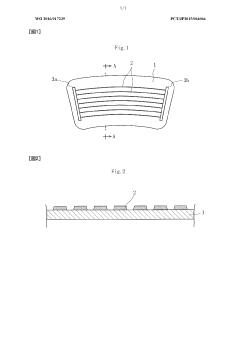
- A crystal-oriented film comprising tungsten-oxygen octahedral blocks with specific crystal orientations perpendicular and parallel to the film surface, utilizing a layered crystal structure and soft chemical treatment to achieve high conductivity and transparency, and incorporating oxygen vacancies to enhance conductive properties.
Environmental Impact of Tungsten Processing
The environmental impact of tungsten processing is a critical consideration in the quest to maximize its conductive properties. Tungsten extraction and refinement processes involve several stages that can have significant ecological consequences. Mining operations, particularly open-pit mining, lead to land degradation, habitat destruction, and potential soil and water contamination. The extraction process often requires large amounts of water, which can strain local water resources and potentially lead to water pollution if not properly managed.
During the ore processing stage, the use of chemicals for separation and purification can result in the release of harmful substances into the environment. These may include heavy metals and other toxic compounds that can persist in ecosystems long after mining operations have ceased. The energy-intensive nature of tungsten processing also contributes to increased carbon emissions, particularly when fossil fuels are the primary energy source.
Waste management is another crucial environmental concern in tungsten processing. Tailings, the residual materials left after ore extraction, can contain hazardous substances and pose risks to surrounding ecosystems if not properly contained. Improper disposal of these wastes can lead to acid mine drainage, a phenomenon where acidic water laden with heavy metals leaches into surrounding soil and water bodies, causing long-term environmental damage.
The refining process of tungsten, which involves high-temperature treatments, can release air pollutants such as sulfur dioxide and particulate matter. These emissions can contribute to air quality degradation and potentially impact human health in surrounding communities. Additionally, the transportation of raw materials and finished products adds to the carbon footprint of tungsten processing.
To mitigate these environmental impacts while maximizing tungsten's conductive properties, several strategies can be employed. Implementing cleaner production technologies and more efficient extraction methods can reduce waste generation and resource consumption. Recycling and reusing process water can help conserve water resources and minimize pollution. Adopting renewable energy sources for processing operations can significantly reduce carbon emissions associated with tungsten production.
Furthermore, investing in research and development of more environmentally friendly extraction and refining techniques is crucial. This may include exploring bio-based extraction methods or developing new chemical processes that are less harmful to the environment. Implementing comprehensive environmental management systems and adhering to strict regulatory standards can also help minimize the ecological footprint of tungsten processing operations.
Applications of High-Conductivity Tungsten
High-conductivity tungsten finds extensive applications across various industries due to its exceptional electrical and thermal properties. In the electronics sector, it serves as a crucial material for manufacturing high-performance semiconductors and integrated circuits. The enhanced conductivity of tungsten enables faster signal transmission and improved heat dissipation in electronic devices, leading to increased efficiency and reliability.
In the lighting industry, high-conductivity tungsten is widely used in the production of filaments for incandescent and halogen lamps. The improved conductivity allows for brighter illumination and longer-lasting bulbs, contributing to energy efficiency and cost-effectiveness in lighting solutions.
The aerospace and defense sectors also benefit from high-conductivity tungsten applications. It is utilized in the fabrication of heat shields, rocket nozzles, and other components that require excellent thermal management capabilities. The material's ability to withstand extreme temperatures while maintaining high conductivity makes it ideal for these demanding environments.
In the field of nuclear energy, high-conductivity tungsten plays a vital role in reactor components and radiation shielding. Its superior heat transfer properties and resistance to radiation damage make it an essential material for ensuring the safety and efficiency of nuclear power plants.
The automotive industry leverages high-conductivity tungsten in the production of high-performance engine components, such as valve stems and piston rings. These parts benefit from improved heat dissipation and wear resistance, contributing to enhanced engine efficiency and longevity.
In the medical field, high-conductivity tungsten is employed in the manufacture of X-ray tubes and radiation therapy equipment. Its excellent thermal and electrical properties enable the production of more precise and efficient medical imaging and treatment devices.
The telecommunications industry utilizes high-conductivity tungsten in the fabrication of microwave and radio frequency components. Its superior conductivity allows for improved signal transmission and reduced power loss in communication systems.
As research and development in materials science continue to advance, new applications for high-conductivity tungsten are likely to emerge, further expanding its importance across various technological domains.