

What Are The Key Materials in Chiplet Integration Processes
OCT 15, 20259 MIN READ
Generate Your Research Report Instantly with AI Agent
PatSnap Eureka helps you evaluate technical feasibility & market potential.
Chiplet Integration Background and Objectives
The semiconductor industry has witnessed a paradigm shift in recent years, moving from traditional monolithic system-on-chip (SoC) designs toward chiplet-based architectures. This transition represents a fundamental change in how integrated circuits are conceptualized, designed, and manufactured. Chiplet technology emerged as a response to the slowing of Moore's Law and the increasing challenges associated with manufacturing large, complex dies with high yields.
Historically, semiconductor advancement followed a predictable path of shrinking transistor sizes and increasing integration. However, as process nodes approached physical limits, the industry encountered diminishing returns in terms of performance gains, power efficiency, and manufacturing costs. The concept of disaggregating complex SoCs into smaller, more manageable chiplets emerged as a viable alternative to traditional scaling approaches around 2015-2017, with AMD's Zen architecture representing one of the first major commercial implementations.
The fundamental principle behind chiplet integration involves partitioning complex systems into smaller functional blocks (chiplets) that can be manufactured separately using optimal process technologies, then integrated onto a common substrate or interposer. This approach allows for mixing and matching of components from different process nodes, vendors, and even different semiconductor technologies, enabling unprecedented flexibility in system design.
Materials science plays a critical role in enabling effective chiplet integration. The interconnect technologies, substrate materials, and bonding methodologies collectively determine the performance, reliability, and cost-effectiveness of chiplet-based systems. As the industry continues to advance, new materials and integration techniques are being developed to address challenges related to thermal management, signal integrity, and manufacturing yield.
The primary objectives of chiplet integration technology development include: reducing manufacturing costs through improved yields and process optimization; enabling heterogeneous integration of diverse components; improving system performance through optimized interconnects; enhancing power efficiency through targeted process selection; and facilitating more flexible product development cycles. Additionally, chiplet integration aims to extend the economic benefits of semiconductor scaling beyond what traditional monolithic approaches can achieve.
Looking forward, the evolution of chiplet integration materials and processes is expected to enable increasingly complex systems with higher performance, lower power consumption, and improved cost structures. This technology trajectory aligns with industry needs for specialized computing solutions across various domains including high-performance computing, artificial intelligence, edge computing, and mobile applications.
Market Demand Analysis for Chiplet Technology
The chiplet integration market is experiencing unprecedented growth driven by the limitations of traditional monolithic chip designs. As Moore's Law faces physical and economic constraints, chiplet technology has emerged as a viable solution for continued performance scaling. Market research indicates that the global chiplet market is projected to grow at a compound annual growth rate of 40% from 2023 to 2030, reaching approximately 50 billion dollars by the end of the decade.
This remarkable growth is primarily fueled by increasing demand for high-performance computing applications across multiple sectors. Data centers and cloud service providers are seeking more efficient solutions to handle exponentially growing computational workloads while managing power consumption and thermal challenges. The chiplet approach allows for optimized performance-per-watt metrics that traditional monolithic designs cannot achieve at advanced nodes.
Consumer electronics manufacturers represent another significant market segment driving chiplet adoption. As smartphones, tablets, and other personal devices require more processing power while maintaining battery efficiency, chiplet-based designs offer compelling advantages. Market analysis shows that consumer electronics could account for nearly 30% of the total chiplet market by 2025.
Automotive and industrial applications are emerging as rapidly growing segments for chiplet technology. Advanced driver-assistance systems (ADAS) and autonomous driving capabilities demand unprecedented computational power in constrained environments. The modularity of chiplet designs allows automotive manufacturers to customize solutions while maintaining reliability standards. This sector is expected to see the fastest growth rate among all chiplet applications over the next five years.
The geographical distribution of chiplet demand shows interesting patterns. North America currently leads in adoption, primarily due to the concentration of hyperscale data centers and advanced semiconductor companies. However, Asia-Pacific is projected to become the largest market by 2026, driven by aggressive investments in semiconductor manufacturing capabilities in Taiwan, South Korea, and China.
From a materials perspective, market demand is creating specific requirements for chiplet integration processes. Advanced packaging materials that can support high-density interconnects while managing thermal challenges are seeing particularly strong demand growth. Silicon interposers, organic substrates with embedded bridges, and advanced dielectric materials are experiencing supply constraints as manufacturers scale up production to meet market needs.
The economic value proposition of chiplet technology is compelling. Industry analysis suggests that chiplet-based designs can reduce development costs by up to 25% compared to monolithic approaches at advanced nodes, while improving time-to-market by approximately 30%. These economic drivers are accelerating adoption across multiple industry verticals despite the initial integration challenges.
Current State and Challenges in Chiplet Integration Materials
Chiplet integration technology has evolved significantly over the past decade, with materials science playing a crucial role in its advancement. Currently, the global chiplet integration materials landscape is characterized by rapid innovation but faces substantial technical barriers. Leading semiconductor manufacturers in the United States, Taiwan, South Korea, and Japan dominate the development of advanced materials for chiplet integration, while China and Europe are making strategic investments to close the gap.
The primary materials challenge in chiplet integration revolves around the interconnect technologies. Traditional solder bumps are reaching their limits in terms of pitch density and thermal performance. Advanced micro-bumps using copper pillars with solder caps have improved electrical performance but still face reliability issues under thermal cycling. Hybrid bonding materials, particularly dielectrics and metal pads, require extreme precision in surface preparation and contamination control, presenting significant manufacturing challenges.
Underfill materials, essential for mechanical stability and thermal management, are struggling to meet the requirements for increasingly dense interconnects. Current underfill formulations face challenges in flow characteristics for ultra-fine pitch applications and often create stress-related reliability issues. Additionally, thermal interface materials (TIMs) are critical but insufficient for managing the concentrated heat generated in high-performance chiplet designs.
Die attach materials present another significant challenge, with traditional adhesives lacking the thermal conductivity required for advanced chiplet packages. Metal sintering materials offer improved thermal performance but face process complexity and cost barriers to widespread adoption. The industry is also grappling with the development of redistribution layer (RDL) materials that can support the increasing electrical, thermal, and mechanical demands of advanced chiplet packages.
Environmental concerns and regulatory pressures are driving the need for lead-free and halogen-free materials throughout the chiplet integration process. This transition has created additional technical challenges, particularly in achieving comparable reliability to traditional materials. Furthermore, the supply chain for critical materials faces significant constraints, with certain rare elements and specialized compounds controlled by a limited number of suppliers.
Manufacturing yield remains a persistent challenge, with material-related defects accounting for a substantial percentage of failures in chiplet integration. Particle contamination, material interface incompatibilities, and process variations contribute to these yield issues. The industry is actively pursuing advanced inspection and metrology techniques to address these challenges, but material innovation remains the fundamental requirement for overcoming current limitations in chiplet integration technology.
Current Material Solutions for Chiplet Integration
01 Interconnect technologies for chiplet integration
Various interconnect technologies are used to connect multiple chiplets in a package. These include advanced packaging techniques such as silicon interposers, bridge chips, and through-silicon vias (TSVs) that enable high-bandwidth, low-latency communication between chiplets. These interconnect solutions address challenges in signal integrity, power delivery, and thermal management while facilitating heterogeneous integration of chiplets manufactured using different process technologies.- Advanced Interconnect Technologies for Chiplet Integration: Various interconnect technologies are employed to enable efficient communication between chiplets in multi-die systems. These include through-silicon vias (TSVs), micro-bumps, and advanced packaging techniques that facilitate high-bandwidth, low-latency connections between different chiplets. These interconnect solutions address challenges related to signal integrity, power delivery, and thermal management in heterogeneous integration scenarios.
- Heterogeneous Integration of Chiplets: Heterogeneous integration involves combining chiplets manufactured using different process technologies or having different functionalities into a single package. This approach allows for optimizing each component separately while achieving system-level performance improvements. The integration may involve combining logic chiplets with memory, analog/RF components, or specialized accelerators to create customized system-on-chip solutions with enhanced capabilities.
- Thermal Management Solutions for Chiplet Architectures: Effective thermal management is critical in chiplet-based designs due to high power densities and potential hotspots at interconnect interfaces. Solutions include advanced thermal interface materials, integrated heat spreaders, and active cooling techniques specifically designed for multi-die packages. These approaches help maintain optimal operating temperatures across all chiplets, ensuring reliability and consistent performance of the integrated system.
- Design and Testing Methodologies for Chiplet-Based Systems: Specialized design and testing methodologies are required for chiplet-based systems to ensure proper functionality and performance. These include pre-silicon validation techniques, design-for-test approaches specific to multi-die integration, and post-packaging testing methods. Advanced EDA tools support chiplet-to-chiplet interface design, system-level optimization, and verification of complex chiplet-based architectures.
- Standardization and Interoperability Frameworks for Chiplets: Industry standards and interoperability frameworks are being developed to facilitate the integration of chiplets from different vendors. These standards define common interfaces, protocols, and physical specifications that enable chiplets to work together seamlessly. Standardization efforts aim to create an ecosystem where chiplets can be mixed and matched like building blocks, reducing development costs and accelerating time-to-market for complex semiconductor products.
02 Thermal management in chiplet architectures
Thermal management is critical in chiplet-based designs due to the high power density and potential hotspots at interconnect interfaces. Solutions include integrated heat spreaders, thermal interface materials specifically designed for chiplet packages, and active cooling techniques. Advanced thermal management approaches consider the unique thermal profiles of heterogeneous chiplets and optimize heat dissipation pathways to maintain performance and reliability in multi-chiplet systems.Expand Specific Solutions03 Power delivery networks for chiplet systems
Specialized power delivery networks are designed to address the unique requirements of chiplet-based architectures. These include integrated voltage regulators, distributed power delivery systems, and advanced power management techniques that optimize power distribution across multiple chiplets. The power delivery solutions account for different voltage domains, minimize IR drop across interconnects, and ensure stable power supply to maintain performance consistency across all chiplets in the system.Expand Specific Solutions04 Testing and yield optimization for chiplet integration
Testing methodologies specific to chiplet-based designs focus on both pre-integration testing of individual chiplets and post-integration system-level testing. These approaches include known-good-die testing, built-in self-test circuits for interconnects, and specialized test structures for evaluating chiplet interfaces. Yield optimization strategies leverage the modularity of chiplet designs to improve overall system yield by selectively combining tested chiplets and implementing redundancy schemes.Expand Specific Solutions05 Design automation and standardization for chiplet ecosystems
Design automation tools and standardization efforts are emerging to support chiplet-based system design. These include specialized EDA tools for chiplet placement and routing, interface protocol standards for chiplet communication, and design methodologies that facilitate chiplet reuse across different products. Standardization initiatives aim to create an open chiplet ecosystem where chiplets from different vendors can be seamlessly integrated, reducing design complexity and time-to-market for chiplet-based systems.Expand Specific Solutions
Major Players in Chiplet Integration Ecosystem
The chiplet integration market is experiencing rapid growth, currently transitioning from early adoption to mainstream implementation phase. The market is projected to expand significantly as heterogeneous integration becomes essential for advanced computing solutions. Leading semiconductor manufacturers like TSMC, SMIC, and Intel are advancing key materials technologies for chiplet integration, with TSMC demonstrating the most mature solutions through their CoWoS and InFO packaging platforms. Materials innovation is being driven by both IDMs and specialized suppliers, with Applied Materials, IBM, and Micron developing advanced interconnect materials, dielectrics, and thermal interface solutions. The competitive landscape shows collaboration between foundries, equipment suppliers, and materials specialists, with increasing investment in research partnerships with institutions like Tsinghua University and Northwestern University to overcome technical challenges in die-to-die interfaces and heterogeneous material integration.
Taiwan Semiconductor Manufacturing Co., Ltd.
Technical Solution: TSMC has pioneered advanced chiplet integration processes through their CoWoS (Chip-on-Wafer-on-Substrate) and InFO (Integrated Fan-Out) packaging technologies. Their CoWoS platform utilizes silicon interposers with through-silicon vias (TSVs) and redistribution layers (RDLs) to connect multiple chiplets. TSMC has developed specialized dielectric materials with low-k properties to minimize signal interference between interconnects. Their latest CoWoS-S technology incorporates high-density interconnects with sub-10μm pitch RDLs and uses proprietary molding compounds that provide thermal stability up to 260°C during reflow processes. TSMC has also developed specialized copper pillar bumps with pitch sizes below 40μm, utilizing advanced solder compositions with controlled intermetallic compound formation to ensure reliable connections between chiplets and the interposer.
Strengths: Industry-leading interconnect density with sub-10μm RDL pitch; superior thermal management materials allowing for higher processing temperatures; established high-volume manufacturing capability. Weaknesses: Higher manufacturing costs compared to traditional packaging; silicon interposer size limitations that constrain maximum chiplet integration scale; longer development cycles for new material integration.
Applied Materials, Inc.
Technical Solution: Applied Materials has developed comprehensive material solutions for chiplet integration through their Advanced Packaging Development Center. Their portfolio includes specialized dielectric materials for redistribution layers with ultra-low-k properties (k<2.5) that minimize signal crosstalk in high-density interconnects. They've pioneered hybrid bonding materials that enable direct copper-to-copper connections with bond strengths exceeding 20 MPa while maintaining electrical performance. Applied Materials' SmartFill technology provides void-free copper filling of high aspect ratio through-silicon vias (TSVs) using specialized plating chemistries and additives that control copper grain structure. Their Endura platform incorporates advanced barrier and seed layer materials, including titanium nitride and ruthenium compounds, that prevent copper diffusion while maintaining excellent adhesion properties. Additionally, they've developed specialized CMP (Chemical Mechanical Planarization) slurries with selective removal rates for different materials, enabling the precise surface preparation required for hybrid bonding processes.
Strengths: Comprehensive material ecosystem covering the entire chiplet integration process flow; established equipment and material co-optimization capabilities; strong expertise in scaling materials for high-volume manufacturing. Weaknesses: Dependent on adoption of specific process flows by foundry partners; some advanced materials require specialized equipment, increasing overall implementation costs; longer qualification cycles for novel materials in high-reliability applications.
Key Material Innovations and Patents in Chiplet Integration
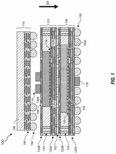
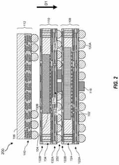
3D chiplet integration using fan-out wafer-level packaging
PatentPendingUS20240274587A1
Innovation
- The use of fan-out wafer-level packaging and three-dimensional packaging techniques for combining semiconductor chips and embedded memory in configurations such as face-to-back, back-to-back, and face-to-face orientations, enabling direct connections between chiplets and reducing assembly package sizes and manufacturing complexity.
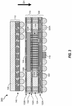
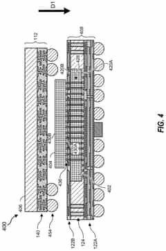
Hybrid bonded interconnect bridging
PatentActiveUS12107075B2
Innovation
- The use of a hybrid bond, comprising a copper bond and an oxide bond, for direct interconnect die coupling to chiplets, enabling finer pitch connections less than 10 micrometers, along with trans-silicon via connections, conductive pillars, and fluorosilicate glass dielectric layers for improved signal transfer and power distribution.
Supply Chain Analysis for Critical Chiplet Materials
The global chiplet integration supply chain represents a complex ecosystem of materials suppliers, manufacturers, and technology providers. Critical materials for chiplet integration include advanced substrates, interposers, micro-bumps, underfill materials, and thermal interface materials. These components form the foundation of heterogeneous integration technologies that enable next-generation computing architectures.
Silicon interposers remain a cornerstone material, with production concentrated in East Asia, particularly Taiwan and South Korea. TSMC controls approximately 65% of the advanced silicon interposer market, creating potential supply vulnerabilities. The organic substrate supply chain is more diversified geographically, with significant production capacity in Japan, South Korea, and increasingly in North America, though specialized high-density substrates face periodic shortages.
Micro-bump materials, particularly copper pillars and solder materials, represent another critical supply chain segment. The refined metals market for these components is relatively stable, but specialized formulations for ultra-fine pitch applications face limited supplier options. Leading suppliers include Tanaka Kikinzoku Kogyo (Japan), Indium Corporation (USA), and Henkel (Germany), collectively controlling over 70% of the high-performance micro-bump materials market.
Underfill and molding compounds present unique supply chain challenges due to their complex chemical formulations and stringent performance requirements. These materials must maintain reliability while accommodating increasingly dense interconnects. The supply chain is dominated by Japanese and American specialty chemical companies, with emerging competition from Chinese manufacturers focusing on cost-competitive alternatives.
Thermal interface materials (TIMs) have become increasingly critical as chiplet designs drive higher thermal densities. The supply chain for advanced TIMs remains concentrated among specialty materials providers, with limited alternatives for highest-performance applications. This segment has experienced periodic supply constraints during demand surges.
Recent geopolitical tensions and pandemic-related disruptions have exposed vulnerabilities in the chiplet materials supply chain. Companies are increasingly implementing multi-sourcing strategies and regional manufacturing diversification to mitigate these risks. The U.S. CHIPS Act and similar initiatives in Europe aim to rebalance the geographic distribution of critical materials production, though meaningful capacity shifts will require 3-5 years of development.
Material qualification cycles represent another supply chain challenge, as new suppliers typically require 12-18 months of validation before integration into production processes. This creates significant barriers to rapid supply chain diversification during shortage situations.
Environmental Impact of Chiplet Integration Materials
The environmental impact of materials used in chiplet integration processes is becoming increasingly significant as the semiconductor industry expands. Traditional packaging materials like lead-based solders have been largely phased out due to their toxicity, replaced by lead-free alternatives such as tin-silver-copper (SAC) alloys. However, these alternatives often require higher processing temperatures, resulting in increased energy consumption during manufacturing.
Organic substrates used in chiplet integration, typically composed of epoxy resins and fiberglass, present environmental challenges related to their non-biodegradable nature and difficult recycling processes. The production of these materials involves petroleum-based chemicals that contribute to carbon emissions. Additionally, flame retardants added to these substrates often contain halogenated compounds that can persist in the environment.
Advanced interconnect materials like copper pillars and micro-bumps utilize metals that require energy-intensive mining and refining processes. The extraction of rare metals used in specialized interconnects contributes to habitat destruction and water pollution in mining regions. Furthermore, chemical-mechanical polishing processes employed during chiplet integration generate significant amounts of slurry waste containing abrasive particles and chemical additives that require specialized disposal.
Water usage represents another critical environmental concern in chiplet manufacturing. The production of ultra-pure water necessary for cleaning processes during integration consumes substantial energy and generates wastewater containing various chemicals and metals. Recent industry initiatives have focused on developing closed-loop water recycling systems to reduce consumption by up to 50% compared to traditional methods.
The underfill and encapsulation materials, typically epoxy-based polymers with silica fillers, present end-of-life disposal challenges due to their durability and resistance to environmental degradation. These materials are designed to protect chiplets from moisture and mechanical stress but consequently become difficult to separate during recycling processes.
Several industry leaders have begun implementing more sustainable practices, including the development of bio-based substrate materials derived from renewable resources. These materials aim to reduce the carbon footprint associated with traditional petroleum-based substrates while maintaining necessary performance characteristics. Additionally, research into halogen-free flame retardants and water-soluble temporary bonding materials shows promise for reducing the environmental impact of chiplet integration processes.
Unlock deeper insights with PatSnap Eureka Quick Research — get a full tech report to explore trends and direct your research. Try now!
Generate Your Research Report Instantly with AI Agent
Supercharge your innovation with PatSnap Eureka AI Agent Platform!