OLED vs MicroLED: Breakthroughs in Semiconductor Design
OCT 24, 20259 MIN READ
Generate Your Research Report Instantly with AI Agent
Patsnap Eureka helps you evaluate technical feasibility & market potential.
Display Technology Evolution and Objectives
Display technology has undergone remarkable evolution since the introduction of cathode ray tubes (CRTs) in the early 20th century. The progression from CRTs to liquid crystal displays (LCDs) marked the first major shift toward flatter, more energy-efficient screens. This transition was followed by the development of plasma display panels, which offered improved contrast ratios and viewing angles but suffered from high power consumption and screen burn-in issues.
The introduction of Organic Light-Emitting Diode (OLED) technology in the late 1990s represented a paradigm shift in display technology. Unlike LCDs that require backlighting, OLED pixels emit light independently when electrical current passes through organic compounds. This self-emissive property enables perfect blacks, infinite contrast ratios, and thinner form factors, making OLEDs particularly suitable for mobile devices and premium televisions.
Despite OLED's advantages, several limitations have driven the search for alternative technologies. These include relatively short lifespans, susceptibility to burn-in (especially with blue subpixels), and manufacturing challenges that impact yield rates and production costs. Additionally, OLED brightness levels, while improving, still lag behind some competing technologies for high-brightness applications.
MicroLED emerged as a promising next-generation display technology, combining the self-emissive properties of OLED with the durability and brightness capabilities of inorganic materials. Based on microscopic LED arrays, this technology offers theoretical advantages including superior brightness (up to 30 times brighter than OLED), longer lifespan (potentially 100,000+ hours), faster response times (nanoseconds versus microseconds), and improved energy efficiency.
The semiconductor design breakthroughs driving both technologies reflect different approaches to similar challenges. OLED development has focused on improving organic material stability, enhancing electron transport layers, and refining thin-film transistor (TFT) backplanes. Meanwhile, MicroLED innovation centers on miniaturization techniques, mass transfer processes, and pixel architecture that maintains efficiency at microscopic scales.
Current technical objectives in the field include achieving cost-effective mass production of MicroLED displays, extending OLED lifespans (particularly for blue subpixels), improving energy efficiency across all display sizes, and developing flexible/foldable form factors. Additionally, researchers aim to enhance color gamut coverage, increase resolution density, and reduce power consumption while maintaining or improving brightness levels.
The evolution trajectory suggests a potential future where these technologies coexist in different market segments, with OLED dominating mid-range consumer electronics and MicroLED establishing presence in premium and specialized applications before potentially achieving broader market penetration as manufacturing costs decrease.
Market Demand Analysis for Advanced Display Technologies
The display technology market is witnessing unprecedented growth driven by increasing consumer demand for superior visual experiences across multiple devices. Current market analysis indicates that the global advanced display market is projected to reach $167 billion by 2025, with OLED technology currently dominating premium segments while MicroLED emerges as a promising contender. This growth trajectory is supported by expanding applications in smartphones, televisions, wearables, automotive displays, and augmented/virtual reality devices.
Consumer preferences are shifting decisively toward thinner, more energy-efficient displays with higher resolution, better color accuracy, and longer lifespans. OLED technology has established strong market penetration in high-end smartphones and premium televisions, with manufacturers like Samsung and LG leading adoption. Meanwhile, MicroLED is gaining traction in luxury televisions and specialized commercial applications where its superior brightness and longevity justify the higher production costs.
The automotive sector represents a particularly promising growth area for advanced display technologies. Modern vehicles increasingly incorporate multiple displays for instrument clusters, infotainment systems, and passenger entertainment. Here, the extreme durability and brightness of MicroLED offer compelling advantages for dashboard displays that must perform reliably under varying lighting conditions, while OLED's flexibility enables innovative curved display implementations.
Regional analysis reveals differentiated market dynamics, with Asia-Pacific leading manufacturing capacity and technological innovation, particularly in South Korea, Japan, and Taiwan. North America and Europe represent significant consumer markets with higher willingness to pay premium prices for advanced display technologies, especially in professional and gaming applications where visual performance is paramount.
Industry forecasts suggest that while OLED will maintain market dominance in the near term due to established manufacturing infrastructure and decreasing production costs, MicroLED is positioned for accelerated growth as manufacturing challenges are overcome. The compound annual growth rate for MicroLED is expected to exceed 80% through 2026, albeit from a smaller base, compared to OLED's more mature 15-20% growth rate.
Supply chain considerations are increasingly influencing market dynamics, with recent semiconductor shortages highlighting vulnerabilities in the display technology ecosystem. Manufacturers are responding by diversifying supplier relationships and investing in vertical integration strategies to secure critical components for both OLED and emerging MicroLED production lines.
Consumer awareness of display technology differences is growing, with purchasing decisions increasingly influenced by technical specifications beyond simple resolution metrics. This trend favors technologies that can deliver measurable improvements in brightness, contrast ratio, color gamut, and energy efficiency – areas where both OLED and MicroLED offer distinct advantages over conventional LCD displays.
OLED and MicroLED Current Status and Technical Barriers
OLED technology has reached commercial maturity with widespread adoption in smartphones, TVs, and wearable devices. Current OLED displays offer excellent color reproduction, perfect black levels, and flexible form factors. Leading manufacturers like Samsung and LG Display have achieved mass production capabilities with yields exceeding 80% for small to medium displays. However, OLED still faces significant technical barriers including limited lifetime (particularly for blue emitters), burn-in susceptibility, and brightness limitations compared to competing technologies.
The manufacturing process for OLED remains complex and costly, requiring precise deposition of organic materials in vacuum environments. Current production methods struggle with uniformity at larger screen sizes, contributing to higher costs for large-format displays. Water and oxygen sensitivity of organic materials necessitates sophisticated encapsulation techniques, adding further complexity to the manufacturing process.
MicroLED technology, while promising, remains in early commercialization stages with limited product availability primarily in premium large-format displays. The technology demonstrates superior brightness (up to 5,000 nits), longer lifetime (100,000+ hours), and better energy efficiency than OLED. MicroLED also offers perfect black levels and wide color gamut comparable to OLED while eliminating burn-in concerns.
The primary technical barrier for MicroLED is mass transfer - the process of precisely placing millions of microscopic LED chips onto a substrate. Current yield rates for this process remain below commercially viable levels for mass-market applications. The industry is exploring various approaches including pick-and-place methods, fluid assembly, and laser transfer techniques, but none have yet achieved the speed and accuracy required for cost-effective production of high-resolution displays.
Size reduction represents another significant challenge, with current microLED chips measuring 10-50 micrometers. Further miniaturization is necessary to achieve the pixel densities required for smartphone and AR/VR applications. Additionally, the technology faces efficiency droop issues at lower currents and challenges in achieving consistent performance across red, green, and blue emitters.
Geographically, OLED development and production is concentrated in East Asia, particularly South Korea and Japan, with emerging capacity in China. MicroLED research shows a broader distribution with significant activity in North America (Apple, Lumileds), Europe (Aledia, Plessey), and Asia (Samsung, Sony). The technology ecosystem includes semiconductor manufacturers, display companies, and specialized equipment providers, creating a complex supply chain that presents both integration challenges and opportunities for innovation.
Current Semiconductor Design Solutions for Display Technologies
01 OLED Display Panel Design and Fabrication
OLED display panels incorporate organic light-emitting diodes that emit light when current flows through them. The semiconductor design for OLEDs focuses on thin-film transistor (TFT) backplanes that control each pixel individually. These designs often include specialized pixel circuits, electrode configurations, and organic material layers to achieve high efficiency, brightness, and color accuracy. Advanced OLED designs may incorporate flexible substrates, transparent components, or foldable architectures to enable new form factors for display applications.- OLED Display Panel Design and Fabrication: OLED (Organic Light Emitting Diode) display panels require specific semiconductor designs to achieve optimal performance. These designs include specialized pixel structures, thin-film transistor arrays, and organic material layers that enable self-illumination. The fabrication process involves precise deposition of organic materials and encapsulation techniques to prevent degradation. Advanced OLED designs incorporate flexible substrates and transparent electrodes to enable bendable and transparent display applications.
- MicroLED Manufacturing and Integration Technologies: MicroLED technology involves the fabrication and integration of microscopic LED arrays into display panels. The semiconductor design focuses on creating ultra-small LED structures with high efficiency and brightness. Manufacturing processes include mass transfer techniques to place millions of tiny LEDs precisely onto substrates. Integration technologies address challenges such as electrical interconnection, thermal management, and yield improvement. These designs enable high brightness, energy efficiency, and pixel density for next-generation displays.
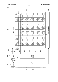
- Semiconductor Backplane Architectures for Display Technologies: Backplane architectures form the foundation of both OLED and MicroLED displays, providing the driving circuitry for pixel control. These designs incorporate thin-film transistor arrays, driving circuits, and addressing schemes to control individual pixels. Advanced backplane technologies include low-temperature polysilicon (LTPS), oxide semiconductors, and silicon-based designs that enable high refresh rates and resolution. The semiconductor design focuses on minimizing power consumption while maximizing display performance through optimized transistor structures and circuit layouts.
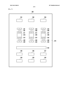
- Pixel Circuit Design for Emissive Displays: Pixel circuit designs for OLED and MicroLED displays require specialized semiconductor architectures to address unique challenges such as current driving, uniformity, and compensation mechanisms. These circuits incorporate transistors, capacitors, and control lines to regulate the current flowing through each emissive element. Advanced designs include compensation circuits that mitigate threshold voltage variations and aging effects. The semiconductor design focuses on achieving uniform brightness, high contrast ratios, and extended operational lifetimes through optimized circuit topologies.
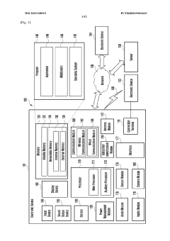
- Integration of Driver ICs and Control Systems: The integration of driver integrated circuits (ICs) and control systems is crucial for OLED and MicroLED display performance. These semiconductor designs include source drivers, gate drivers, timing controllers, and power management circuits that work together to deliver precise signals to the display panel. Advanced integration approaches include chip-on-glass (COG), chip-on-film (COF), and system-on-chip (SoC) technologies that reduce form factor and improve reliability. The semiconductor design focuses on high-speed data processing, efficient power delivery, and seamless communication between components.
02 MicroLED Manufacturing Processes and Integration
MicroLED technology involves the fabrication and integration of microscopic inorganic LED arrays into display panels. The semiconductor design challenges include mass transfer techniques to position tiny LED chips accurately, electrical interconnection methods, and addressing schemes. Manufacturing processes may involve epitaxial growth of LED structures, wafer bonding, and pick-and-place technologies. Integration approaches focus on combining the microLED elements with driving circuits while maintaining high yield and reliability despite the miniaturized scale of components.Expand Specific Solutions03 Driving Circuit Architectures for Advanced Displays
Specialized driving circuit architectures are essential for controlling OLED and MicroLED displays. These semiconductor designs include pixel driving circuits, gate drivers, data drivers, and timing controllers optimized for the unique electrical characteristics of each display technology. Advanced architectures may incorporate compensation schemes for device aging, current programming methods for uniform brightness, or pulse width modulation techniques for precise grayscale control. The integration density and power efficiency of these circuits directly impact the overall display performance and energy consumption.Expand Specific Solutions04 Thermal Management and Reliability Solutions
Thermal management is critical in both OLED and MicroLED semiconductor designs due to heat generation during operation. Solutions include specialized substrate materials with high thermal conductivity, heat dissipation structures, and temperature sensing circuits. Reliability enhancements focus on preventing degradation mechanisms such as pixel aging in OLEDs or interconnect failures in MicroLEDs. Design approaches may incorporate redundant elements, encapsulation techniques to prevent moisture ingress, or compensation algorithms to maintain consistent performance over the device lifetime.Expand Specific Solutions05 Hybrid and Novel Display Architectures
Innovative semiconductor designs explore hybrid architectures that combine elements of OLED and MicroLED technologies or integrate them with other display approaches. These designs may include tandem structures with multiple emission layers, quantum dot color conversion layers, or novel pixel arrangements to optimize efficiency and visual performance. Some architectures focus on specific applications such as augmented reality displays, transparent displays, or ultra-high resolution implementations. Advanced manufacturing techniques enable 3D integration of display elements with sensors or processing components to create multifunctional display systems.Expand Specific Solutions
Key Industry Players in OLED and MicroLED Development
The OLED vs MicroLED display technology landscape is currently in a transitional phase, with OLED reaching maturity while MicroLED remains in early commercialization. The global market for these advanced display technologies is projected to exceed $200 billion by 2025, driven by demand for higher performance displays in consumer electronics and automotive applications. Leading OLED manufacturers like Samsung Display, LG Display, and BOE Technology have established mass production capabilities, while companies including Samsung Electronics, Apple, and TCL are investing heavily in MicroLED development. The technological competition is intensifying as MicroLED promises superior brightness, energy efficiency, and longevity compared to OLED, though manufacturing challenges remain. Companies like Applied Materials and Universal Display are developing critical materials and equipment to advance both technologies.
BOE Technology Group Co., Ltd.
Technical Solution: BOE has developed advanced OLED technologies including flexible AMOLED displays utilizing low-temperature polycrystalline oxide (LTPO) backplane technology that enables variable refresh rates from 1-120Hz, reducing power consumption by up to 20% compared to standard LTPS backplanes[5]. Their OLED panels achieve brightness levels exceeding 1,500 nits with HDR10+ certification. For MicroLED, BOE has pioneered glass-based active-matrix driving technology with integrated circuits that significantly improve current uniformity across MicroLED arrays. Their MicroLED displays feature pixel pitches as small as 0.9mm with contrast ratios exceeding 1,000,000:1[6]. BOE has developed proprietary "micro-IC" architecture that integrates driver ICs directly with MicroLED chips, reducing interconnection complexity and improving reliability. They've also created hybrid transfer techniques combining mechanical and laser-assisted processes to achieve transfer yields above 99.99% for mass production, addressing one of the key challenges in MicroLED manufacturing.
Strengths: Comprehensive display technology portfolio spanning multiple generations; strong vertical integration from materials to finished displays; significant manufacturing scale advantages. Weaknesses: Still catching up to Samsung and LG in premium OLED market segments; MicroLED mass production capabilities remain limited compared to established OLED lines; higher defect rates in cutting-edge display technologies compared to industry leaders.
SAMSUNG DISPLAY CO LTD
Technical Solution: Samsung Display has pioneered significant breakthroughs in both OLED and MicroLED technologies. For OLED, they've developed QD-OLED (Quantum Dot OLED) technology that combines quantum dots with OLED to achieve superior color volume exceeding 100% of DCI-P3 color space and viewing angles up to 175 degrees[1]. Their OLED panels feature pixel densities exceeding 10,000 PPI for AR/VR applications. In MicroLED, Samsung has developed "The Wall" modular MicroLED display system with micrometer-sized LEDs that are 1/100th the size of conventional LEDs, achieving brightness levels up to 2,000 nits while maintaining perfect blacks[2]. Their proprietary low-temperature polycrystalline silicon (LTPS) thin-film transistor (TFT) backplanes enable precise current delivery to individual MicroLEDs. Samsung has also developed mass transfer techniques capable of placing millions of MicroLEDs with sub-micron accuracy, addressing one of the key manufacturing challenges in MicroLED production.
Strengths: Vertical integration from semiconductor manufacturing to display production; proprietary quantum dot color conversion technology; advanced mass transfer techniques for MicroLED. Weaknesses: High production costs for both premium OLED and MicroLED displays; MicroLED manufacturing yield challenges; energy-intensive production processes compared to conventional LCD manufacturing.
Critical Patents and Innovations in OLED and MicroLED
Transfer substrate
PatentInactiveUS20220130707A1
Innovation
- A transfer substrate design featuring a support with a groove portion and an elastic body with projection portions, allowing for the pickup and release of elements through deformation, eliminating the need for large-scale vacuum equipment by creating a closed space for pressure adjustment.
LED display and electronic device having same
PatentWO2019208919A1
Innovation
- The development of a micro-LED display with a bezel-less design and segmentation capabilities, allowing for flexible displays of various sizes, achieved through direct mounting of micro-LEDs on a substrate and innovative electrical connections using conductive patterns and wiring lines, enabling robust electrical connections and flexible display configurations.
Supply Chain Challenges and Manufacturing Scalability
The supply chain for display technologies represents a critical factor in determining market adoption and commercial viability. For OLED technology, the supply chain has matured significantly over the past decade, with established manufacturing processes centered primarily in East Asia. South Korean manufacturers like Samsung and LG Display dominate high-end OLED production, while Chinese companies have rapidly expanded their manufacturing capacity for mid-range applications. However, OLED production continues to face yield challenges, particularly for larger panels, resulting in higher costs and production inefficiencies.
MicroLED faces considerably more complex supply chain challenges. The technology requires precision manufacturing at an unprecedented scale, with millions of microscopic LEDs that must be individually placed with near-perfect accuracy. This mass transfer process represents one of the most significant bottlenecks in the MicroLED supply chain. Current manufacturing techniques struggle to achieve the necessary throughput while maintaining acceptable yields, particularly as display sizes increase and pixel densities grow.
Raw material constraints also differentiate these technologies. OLED production relies heavily on organic materials that have established supply networks but face price volatility. MicroLED requires specialized semiconductor materials and rare earth elements for phosphors, potentially creating supply vulnerabilities as production scales. The geographical concentration of rare earth processing in specific regions introduces geopolitical risks to the MicroLED supply chain.
Manufacturing scalability presents divergent challenges for each technology. OLED has achieved reasonable economies of scale for smaller displays but continues to face yield issues for television-sized panels. The industry has invested billions in expanding OLED manufacturing capacity, though the returns on these investments remain uncertain in some market segments. MicroLED manufacturing, meanwhile, requires entirely new production paradigms and equipment sets that are still being developed.
Equipment suppliers represent another critical link in these supply chains. OLED manufacturing relies on specialized vacuum deposition equipment from companies like Applied Materials and Canon Tokki, with the latter facing persistent order backlogs that constrain industry expansion. MicroLED requires precision placement tools that are still evolving, with companies like ASM Pacific Technology and Kulicke & Soffa developing mass transfer solutions that remain insufficient for truly high-volume manufacturing.
The environmental impact of these supply chains also merits consideration. OLED production involves energy-intensive processes and potentially hazardous chemicals, while MicroLED manufacturing may offer reduced environmental impact per unit but currently suffers from higher material waste due to yield issues. As sustainability becomes increasingly important to consumers and regulators, these factors will influence supply chain development and manufacturing investments.
Energy Efficiency and Sustainability Considerations
Energy efficiency represents a critical differentiator between OLED and MicroLED technologies, with significant implications for both consumer applications and environmental sustainability. OLED displays inherently consume less power when displaying darker content due to their emissive nature, where black pixels are simply turned off. This pixel-level power management gives OLED an advantage in applications with predominantly dark content, such as mobile devices with dark mode interfaces.
MicroLED technology, while still evolving, demonstrates promising energy efficiency characteristics that may eventually surpass OLED. Current research indicates that MicroLED displays can achieve up to 30% higher energy efficiency at maximum brightness levels compared to OLED, primarily due to their superior light emission efficiency and reduced heat generation. This advantage becomes particularly significant in high-brightness applications such as automotive displays and outdoor signage.
Manufacturing sustainability presents another important dimension in comparing these technologies. OLED production currently involves several environmentally challenging processes, including the use of rare earth materials and organic compounds that require careful handling and disposal. The manufacturing process also demands significant energy consumption, particularly during the vacuum deposition phases.
MicroLED manufacturing, while still scaling toward mass production, presents both challenges and opportunities from a sustainability perspective. The technology requires fewer rare earth elements than some competing technologies, but the precision equipment needed for mass transfer processes currently consumes substantial energy. Recent innovations in manufacturing techniques, such as fluidic self-assembly and laser transfer methods, show promise for reducing both material waste and energy consumption.
Lifecycle considerations reveal further distinctions between these technologies. OLED displays typically have shorter operational lifespans due to organic material degradation, particularly in blue subpixels, necessitating more frequent replacement. MicroLED displays theoretically offer significantly longer operational lifetimes—potentially exceeding 100,000 hours compared to OLED's typical 30,000-50,000 hours—which translates to reduced electronic waste over time.
Recycling capabilities also differ substantially between these technologies. OLED panels present recycling challenges due to their multi-layer organic structure and specialized encapsulation materials. MicroLED displays, with their predominantly inorganic composition, may offer improved end-of-life recyclability, though specialized recovery processes for the microscopic LED elements remain under development.
Unlock deeper insights with Patsnap Eureka Quick Research — get a full tech report to explore trends and direct your research. Try now!
Generate Your Research Report Instantly with AI Agent
Supercharge your innovation with Patsnap Eureka AI Agent Platform!