OLED vs MicroLED: Current Patents and Innovations
OCT 24, 20259 MIN READ
Generate Your Research Report Instantly with AI Agent
Patsnap Eureka helps you evaluate technical feasibility & market potential.
Display Technology Evolution and Objectives
Display technology has undergone remarkable evolution since the introduction of cathode ray tubes (CRTs) in the early 20th century. The progression from CRTs to liquid crystal displays (LCDs) marked the first major shift toward flatter, more energy-efficient screens. This transition was followed by the development of plasma display panels, which offered improved contrast ratios and viewing angles but suffered from high power consumption and screen burn-in issues.
The introduction of Organic Light-Emitting Diode (OLED) technology in the late 1990s represented a revolutionary advancement in display technology. Unlike LCDs that require backlighting, OLED pixels emit their own light when an electric current passes through them, enabling thinner displays with superior contrast ratios, faster response times, and better color reproduction. OLED technology has since dominated high-end smartphone and television markets.
MicroLED emerged as a promising next-generation display technology around 2010, combining the self-emissive properties of OLED with the durability and brightness capabilities of inorganic materials. MicroLED displays utilize microscopic LED arrays that individually emit light, potentially offering higher brightness, longer lifespan, and better energy efficiency than OLED displays.
The current competitive landscape between OLED and MicroLED technologies is shaped by significant patent activities and continuous innovations. Samsung and LG Display lead OLED patent portfolios, while Apple, Samsung, and Sony have made substantial investments in MicroLED intellectual property. These patents primarily focus on manufacturing processes, material compositions, and integration techniques.
The technical objectives for both technologies include overcoming specific challenges. For OLED, these involve extending operational lifespan, improving blue pixel efficiency, and reducing production costs. MicroLED faces challenges in mass transfer techniques for placing millions of microscopic LEDs precisely, yield management, and scaling down pixel sizes while maintaining performance.
Industry projections suggest that while OLED will continue dominating the premium display market in the near term, MicroLED is positioned to capture significant market share in specialized applications requiring extreme brightness and durability, such as AR/VR headsets, automotive displays, and large-format public information displays.
The evolution trajectory aims toward displays that combine perfect black levels, infinite contrast ratios, wide color gamuts, high refresh rates, energy efficiency, and form factor flexibility. Both technologies are advancing toward these ideals through different technical approaches, with their respective patent landscapes revealing distinct innovation strategies and technological priorities.
Market Analysis for Advanced Display Technologies
The global display technology market is witnessing a significant shift as advanced technologies like OLED and MicroLED compete for dominance. The display market reached approximately $148 billion in 2022 and is projected to grow at a CAGR of 7.2% through 2030, driven by increasing demand for high-quality displays in consumer electronics, automotive interfaces, and commercial applications.
OLED technology currently holds a substantial market share, particularly in premium smartphones and high-end televisions. Samsung Display and LG Display lead the OLED market with combined revenues exceeding $25 billion annually from OLED panel sales. The OLED TV segment has shown remarkable growth, with shipments increasing by 73% year-over-year in 2022, despite representing only 3% of the total TV market volume.
MicroLED, though still emerging, is gaining significant attention from investors and manufacturers. Market analysts predict MicroLED displays could capture 10% of the premium display market by 2026, with potential applications expanding beyond consumer electronics to automotive displays, augmented reality devices, and large-format commercial displays. Current market penetration remains below 1%, but investment in manufacturing infrastructure has surpassed $4 billion globally in the past three years.
Regional analysis reveals Asia-Pacific dominates display manufacturing, with South Korea, Japan, China, and Taiwan accounting for over 90% of global production capacity. North America and Europe lead in intellectual property development and specialized applications, while emerging markets show increasing demand for mid-range display technologies.
Consumer preference analysis indicates growing demand for higher resolution, improved color accuracy, and energy efficiency across all display applications. The premium smartphone segment shows 67% of consumers willing to pay more for superior display quality, while automotive displays are expected to grow at 15% annually through 2028 as advanced driver assistance systems become standard.
Supply chain considerations reveal potential vulnerabilities, with critical materials like indium facing supply constraints. MicroLED manufacturing requires specialized equipment and processes, creating barriers to rapid market expansion but also opportunities for equipment manufacturers and material suppliers to establish dominant positions in this emerging ecosystem.
Price sensitivity analysis shows OLED has achieved significant cost reductions over the past decade, while MicroLED remains prohibitively expensive for mass-market applications. Industry projections suggest MicroLED manufacturing costs could decrease by 60% by 2027 as production scales and yields improve, potentially accelerating market adoption.
OLED and MicroLED Technical Challenges
Both OLED and MicroLED display technologies face significant technical challenges that impact their commercial viability and market adoption. OLED technology, despite being more mature in the market, continues to struggle with several persistent issues. The organic materials in OLED displays remain susceptible to degradation when exposed to oxygen and moisture, resulting in limited operational lifespans, particularly for blue OLED emitters which typically degrade faster than red and green counterparts.
Manufacturing scalability presents another major challenge for OLED. While small and medium-sized OLED panels have achieved reasonable production yields, large-format displays still face manufacturing difficulties that increase costs significantly. The industry continues to search for more efficient deposition methods beyond the current vacuum thermal evaporation techniques.
Power efficiency remains problematic, especially for mobile applications where battery life is critical. Although OLED displays can be more energy-efficient than LCDs when displaying dark content, they consume considerably more power when displaying bright or white content. This characteristic limits their application in certain scenarios.
MicroLED technology, while promising superior performance in many aspects, faces even more formidable technical hurdles. The most significant challenge is the mass transfer process - efficiently and precisely placing millions of microscopic LED chips onto a display substrate with near-perfect yield. Current approaches include laser transfer, electrostatic transfer, and fluid-assisted methods, but none has yet achieved the combination of speed, accuracy, and cost-effectiveness required for mass production.
Pixel size reduction represents another critical challenge for MicroLED. Creating LED chips small enough for high-resolution displays while maintaining brightness and efficiency is extremely difficult. As the LED size decreases below 10 micrometers, quantum efficiency tends to drop dramatically due to increased surface defects relative to volume.
Color conversion technology also presents obstacles for MicroLED. While blue LEDs are relatively efficient, creating red and green pixels either requires different LED materials or phosphor/quantum dot conversion layers, each approach introducing its own complications regarding efficiency and manufacturing complexity.
Both technologies also face challenges related to backplane technology, with requirements for increasingly sophisticated thin-film transistor arrays to drive individual pixels. Additionally, inspection and repair processes for identifying and addressing defects remain time-consuming and costly, particularly for MicroLED where a single defective pixel can render an entire display unusable.
Current Patent Landscape and Solutions
01 OLED Display Technology Innovations
Organic Light Emitting Diode (OLED) technology has seen significant advancements in display applications. These innovations include improvements in organic materials, pixel structures, and manufacturing processes that enhance brightness, energy efficiency, and display quality. OLED displays offer advantages such as flexibility, thinness, and superior color reproduction compared to traditional display technologies.- OLED Display Technology Innovations: Organic Light Emitting Diode (OLED) technology has seen significant advancements in display applications. These innovations include improvements in organic materials, pixel structures, and manufacturing processes that enhance brightness, energy efficiency, and display quality. OLED displays offer advantages such as flexibility, thinness, and superior color reproduction compared to traditional display technologies.
- MicroLED Display Developments: MicroLED technology represents a breakthrough in display technology, utilizing microscopic LED arrays to create high-resolution displays. Recent innovations focus on manufacturing techniques to overcome production challenges, improving pixel density, and enhancing color accuracy. MicroLED displays offer advantages including higher brightness, better energy efficiency, and longer lifespan compared to other display technologies.
- Display Driver Integration and Control Systems: Advanced driver integration circuits and control systems are crucial for both OLED and MicroLED displays. Innovations in this area include improved backplane technologies, thin-film transistor designs, and signal processing algorithms that enhance display performance. These systems manage power consumption, pixel addressing, and refresh rates to optimize display quality and efficiency.
- Flexible and Foldable Display Technologies: Flexible display technologies have evolved significantly, enabling foldable and rollable screens for various applications. These innovations involve specialized substrate materials, encapsulation techniques, and mechanical designs that allow displays to bend without damage. Such technologies are particularly applicable to mobile devices, wearables, and next-generation consumer electronics.
- Manufacturing Processes and Yield Improvement: Manufacturing innovations for OLED and MicroLED displays focus on improving production efficiency and yield rates. These include advanced deposition techniques, transfer processes for MicroLED chips, and quality control systems. Recent patents address challenges in mass production, cost reduction, and scaling of high-resolution displays for commercial applications.
02 MicroLED Display Developments
MicroLED technology represents a breakthrough in display technology, utilizing microscopic LED arrays to create high-resolution displays. Recent innovations focus on manufacturing techniques to overcome production challenges, improving pixel density, and enhancing color accuracy. MicroLED displays offer advantages including higher brightness, better energy efficiency, and longer lifespan compared to other display technologies.Expand Specific Solutions03 Display Driver Integration and Control Systems
Advanced driver integration circuits and control systems are crucial for both OLED and MicroLED displays. Innovations in this area include improved backplane technologies, thin-film transistor designs, and signal processing algorithms that enhance display performance. These systems manage power consumption, pixel addressing, and refresh rates to optimize display quality and efficiency.Expand Specific Solutions04 Flexible and Foldable Display Technologies
Flexible display technologies have evolved significantly, particularly in OLED and emerging MicroLED applications. These innovations enable displays that can be bent, folded, or rolled while maintaining visual performance. Key developments include flexible substrates, encapsulation methods, and stress-resistant pixel structures that allow for novel form factors in consumer electronics.Expand Specific Solutions05 Energy Efficiency and Power Management
Energy efficiency innovations in display technologies focus on reducing power consumption while maintaining or improving display quality. These advancements include pixel-level power management, adaptive brightness control, and optimized driving schemes. Such innovations are particularly important for battery-powered devices and contribute to the overall sustainability of display technologies.Expand Specific Solutions
Key Industry Players and Competitive Landscape
The OLED vs MicroLED technology landscape is currently in a transitional phase, with OLED being mature and commercially established while MicroLED remains in early commercialization. The global market for these technologies is projected to reach $200+ billion by 2025, driven by demand for superior displays in consumer electronics and automotive applications. In terms of technical maturity, Samsung and LG Display lead OLED commercialization with extensive patent portfolios, while BOE Technology is rapidly advancing. For MicroLED, Samsung, Apple, and Sony are frontrunners in patent development, with companies like Lumileds and eMagin making significant innovations in miniaturization and manufacturing processes. Universal Display Corporation maintains critical IP in OLED materials, while emerging players like TCL and Sharp are increasing their patent activities.
BOE Technology Group Co., Ltd.
Technical Solution: BOE has developed flexible OLED display technology with innovations in thin-film encapsulation and flexible substrates. Their patents cover specialized pixel circuit designs that compensate for TFT threshold voltage variations, improving display uniformity. For smartphone displays, BOE has created under-display camera solutions using transparent OLED areas with modified pixel arrangements. In the MicroLED domain, BOE has focused on developing cost-effective manufacturing processes, including innovations in mass transfer techniques using laser-assisted methods. Their approach involves selective laser energy transfer that enables precise placement of microLED chips onto receiver substrates. BOE has also patented unique pixel structure designs that improve light extraction efficiency and reduce optical crosstalk between adjacent pixels [4][7]. Their recent innovations include specialized phosphor-converted MicroLED technologies that use blue MicroLEDs with color conversion layers to achieve full-color displays with reduced manufacturing complexity. BOE has additionally developed repair techniques for MicroLED displays that allow for individual defective pixels to be replaced after initial assembly, significantly improving manufacturing yields.
Strengths: BOE possesses extensive manufacturing capacity and has rapidly advanced their OLED technology to compete with Korean manufacturers. Their focus on cost-effective manufacturing processes positions them well for eventual MicroLED mass production. Weaknesses: Their OLED technology still lags behind Samsung and LG in some performance metrics like color accuracy and power efficiency. Their MicroLED development remains primarily in research phase with limited commercial products compared to market leaders.
SAMSUNG DISPLAY CO LTD
Technical Solution: Samsung Display has developed advanced OLED technologies including their proprietary Quantum Dot OLED (QD-OLED) panels that combine quantum dot color conversion with OLED light emission. Their technology utilizes blue OLED as the light source with quantum dots converting blue light into red and green, achieving wider color gamut and improved efficiency. For MicroLED, Samsung has pioneered modular MicroLED displays with their "The Wall" product line, featuring individually addressable RGB LED pixels at micrometer scale. Their patent portfolio includes innovations in pixel transfer techniques, where microscopic LED chips are precisely placed on backplane substrates using mass transfer methods. Samsung has also developed unique electrode structures and driving methods to maintain brightness uniformity across large MicroLED panels [1][3]. Their recent innovations focus on reducing pixel pitch to below 100 micrometers while maintaining high brightness and contrast ratios exceeding 1,000,000:1.
Strengths: Samsung holds dominant market position in both OLED and MicroLED with extensive manufacturing infrastructure and vertical integration capabilities. Their QD-OLED technology offers superior color performance compared to conventional OLED. Weaknesses: Their MicroLED technology still faces yield challenges at smaller pixel pitches, and high manufacturing costs limit mass market adoption. Their OLED panels still experience some burn-in issues with static content despite mitigation efforts.
Critical Innovations in Display Technologies
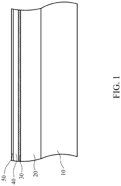
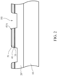
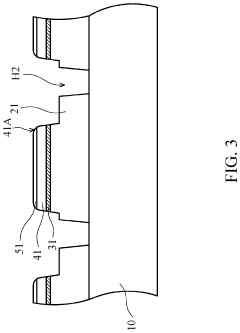
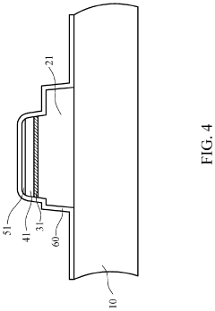
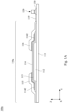
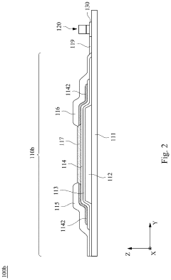
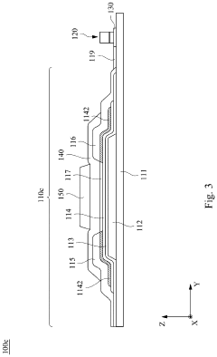
Micro light-emitting diode structure and micro light-emitting diode display device using the same
PatentInactiveUS20220173273A1
Innovation
- A flip-chip micro light-emitting diode structure is designed where the mesa region is smaller than the first-type semiconductor layer, exposing a portion of its top surface for electrode connection, eliminating the need for multiple aligned holes and simplifying the manufacturing process.
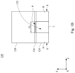
Micro light-emitting diode display device and micro light-emitting diode driving circuit
PatentActiveUS10680035B1
Innovation
- A micro light-emitting diode display device with a driving transistor featuring a gate insulator thickness of less than or equal to 500 angstroms and a micro light-emitting diode with a current injection channel and an active layer portion in contact with the channel, reducing the light-emitting area and avoiding surface recombination, thereby lowering the voltage required to activate the diode.
Manufacturing Process Comparison
The manufacturing processes for OLED and MicroLED displays represent fundamentally different approaches with distinct challenges and advantages. OLED manufacturing has matured significantly over the past decade, utilizing established vapor deposition techniques for organic materials. The process typically involves depositing multiple organic layers onto a substrate through either vacuum thermal evaporation (VTE) for small molecule OLEDs or solution processing for polymer OLEDs. Major manufacturers have achieved economies of scale, with Gen 10.5 fabs now operational, significantly reducing production costs.
In contrast, MicroLED manufacturing remains in earlier development stages, facing considerable challenges in mass transfer processes. The core difficulty lies in precisely transferring millions of microscopic LED chips from a donor substrate to a display backplane with near-perfect yield. Current approaches include stamp transfer, laser-assisted transfer, and fluid-assisted assembly, each with varying degrees of success in research settings.
Patent analysis reveals that Samsung Display and LG Display dominate OLED manufacturing patents, focusing on improving deposition uniformity and reducing material waste. For MicroLED, Apple's acquisition of LuxVue Technology has yielded significant intellectual property around mass transfer techniques, while companies like PlayNitride and X-Celeprint have developed innovative approaches to handling the miniature components.
Yield rates present a stark contrast between technologies. OLED manufacturing has achieved commercial yields exceeding 90% for smartphone displays, whereas MicroLED yields remain problematic, particularly as display resolution increases. Each defective MicroLED pixel requires individual repair, dramatically increasing production costs.
Equipment infrastructure also differs substantially. OLED manufacturing leverages modified semiconductor equipment from established vendors like Applied Materials and Canon Tokki. MicroLED requires specialized equipment still under development, with companies like ASM Pacific Technology and Toray Engineering pioneering new solutions for mass transfer and inspection.
Cost structures reflect these manufacturing differences. OLED production costs have decreased approximately 35% over the past five years through process optimization and economies of scale. MicroLED costs remain prohibitively high for consumer applications, with estimates suggesting production costs 5-8 times higher than equivalent OLED displays, primarily due to complex transfer processes and lower yields.
Environmental considerations also differentiate these technologies. OLED manufacturing involves organic solvents requiring careful handling and disposal, while MicroLED processes use fewer hazardous materials but may have higher energy requirements during production. Recent innovations focus on reducing environmental impact for both technologies through material recycling and energy-efficient equipment design.
Sustainability and Energy Efficiency Factors
The sustainability and energy efficiency comparison between OLED and MicroLED technologies represents a critical factor in their commercial viability and environmental impact. OLED displays currently demonstrate moderate energy efficiency, with power consumption varying significantly based on content displayed. Dark content consumes substantially less power than bright scenes due to OLED's emissive nature where black pixels remain unlit. However, OLED manufacturing processes involve environmentally concerning materials including heavy metals and organic solvents.
Recent patent filings from Samsung Display and LG Display reveal innovations focused on reducing OLED power consumption through pixel structure optimization and more efficient driving methods. These developments aim to address OLED's historical disadvantage in high-brightness scenarios where power consumption escalates dramatically.
MicroLED technology presents promising advancements in energy efficiency, with theoretical power consumption 30-50% lower than comparable OLED displays at equivalent brightness levels. This efficiency stems from MicroLED's superior electroluminescent properties and more direct conversion of electricity to light. Apple's recent patents demonstrate novel approaches to MicroLED power management, including adaptive brightness control systems that optimize energy usage based on ambient conditions and content characteristics.
Manufacturing sustainability represents another critical dimension. Current MicroLED production requires significant energy input and specialized equipment, resulting in a larger initial carbon footprint compared to established OLED manufacturing. However, patent analysis reveals intensive research into more sustainable MicroLED production methods, with Sony and Samsung leading innovations in reduced-temperature manufacturing processes and recycling techniques for rare earth materials.
Longevity factors significantly into overall sustainability calculations. MicroLED's superior lifespan—estimated at 100,000+ hours versus OLED's 30,000-50,000 hours—translates to fewer replacement cycles and reduced electronic waste. This advantage is reinforced by MicroLED's resistance to burn-in effects that plague OLED displays, particularly in commercial applications with static content.
Material recoverability presents contrasting profiles. OLED's organic compounds pose recycling challenges, while MicroLED's inorganic materials offer better theoretical recoverability. However, the complex integration of MicroLED components creates practical recycling obstacles. Recent innovations from LG and BOE Technology focus on modular design approaches that may facilitate future component separation and material recovery.
Energy efficiency certifications increasingly influence market adoption, with both technologies competing to meet stringent Energy Star and TCO requirements. Patent activity indicates manufacturers are prioritizing compliance with these standards, recognizing their growing importance in procurement decisions across consumer, commercial, and industrial applications.
Unlock deeper insights with Patsnap Eureka Quick Research — get a full tech report to explore trends and direct your research. Try now!
Generate Your Research Report Instantly with AI Agent
Supercharge your innovation with Patsnap Eureka AI Agent Platform!