OLED vs MicroLED: Electromagnetic Spectrum Utilization
OCT 24, 20259 MIN READ
Generate Your Research Report Instantly with AI Agent
Patsnap Eureka helps you evaluate technical feasibility & market potential.
Display Technology Evolution and Objectives
Display technology has undergone remarkable evolution since the introduction of cathode ray tubes (CRTs) in the early 20th century. This progression has been characterized by continuous improvements in resolution, color accuracy, energy efficiency, and form factor. The transition from CRTs to liquid crystal displays (LCDs) marked the first major shift toward flatter, more energy-efficient screens. Subsequently, plasma display panels offered improved contrast ratios and viewing angles before being largely superseded by LCD technology enhanced with LED backlighting.
The emergence of OLED (Organic Light-Emitting Diode) technology in the early 2000s represented a paradigm shift in display technology. Unlike LCDs that require backlighting, OLED pixels emit their own light when an electric current is applied, enabling true blacks, higher contrast ratios, and thinner form factors. This self-emissive property fundamentally changed how displays utilize the electromagnetic spectrum, allowing for more precise control of light emission across visible wavelengths.
MicroLED technology, first demonstrated in the early 2010s, represents the next frontier in display evolution. Building on the self-emissive principle of OLEDs, MicroLEDs utilize inorganic semiconductor materials to create microscopic LED arrays that function as individual pixels. This approach promises to overcome several limitations of OLED technology, particularly in terms of brightness, longevity, and energy efficiency.
The electromagnetic spectrum utilization represents a critical differentiator between OLED and MicroLED technologies. OLEDs employ organic compounds that convert electrical energy into light across specific wavelength ranges, with different organic materials responsible for red, green, and blue light emission. This organic nature introduces inherent limitations in spectrum purity, peak brightness, and long-term stability of certain wavelengths, particularly blue.
MicroLEDs, conversely, leverage inorganic semiconductor materials similar to traditional LEDs but at a microscopic scale. These materials can be engineered with greater precision to emit light at very specific wavelengths, resulting in purer colors and potentially wider color gamuts. The inorganic composition also enables significantly higher brightness levels without degradation, allowing for better performance in high ambient light conditions.
The primary technical objective in this domain is to develop display technologies that maximize electromagnetic spectrum utilization efficiency while minimizing energy consumption. This includes achieving wider color gamuts (approaching or exceeding Rec. 2020 standards), higher peak brightness (1,000+ nits for consumer displays), perfect black levels (zero light emission when pixels are off), and minimal color shift over the lifetime of the display.
Additional objectives include reducing manufacturing complexity, enhancing yield rates, and developing scalable production methods that can support various display sizes from smartphone screens to large-format televisions and commercial displays. The ultimate goal is to create display technology that faithfully reproduces the full range of human-visible colors with perfect contrast, while maintaining practical energy consumption levels and competitive production costs.
Market Demand Analysis for Advanced Display Technologies
The display technology market is witnessing unprecedented growth driven by consumer electronics, automotive interfaces, and commercial applications. Current market analysis indicates that the global advanced display market reached approximately $148 billion in 2022 and is projected to grow at a CAGR of 8.2% through 2028. This expansion is primarily fueled by increasing demand for higher resolution, energy-efficient displays with superior color reproduction capabilities.
OLED technology currently dominates the premium smartphone and high-end television segments, with Samsung and LG maintaining significant market share. Consumer preference studies show that 73% of high-end device purchasers consider display quality a critical factor in their buying decisions, with color accuracy and brightness being paramount considerations.
MicroLED technology, though still emerging, is generating substantial market interest due to its potential advantages in brightness, longevity, and energy efficiency. Market forecasts suggest MicroLED displays could capture 15% of the premium display market by 2026, primarily in luxury televisions, high-end wearables, and automotive applications where durability and brightness are essential.
The electromagnetic spectrum utilization difference between these technologies represents a key market differentiator. OLED's self-emissive organic compounds provide excellent color reproduction but with limitations in peak brightness and lifetime. Market research indicates that 68% of professional users prioritize color accuracy, making OLED particularly strong in creative industries and premium consumer segments.
MicroLED's inorganic LED-based approach offers superior brightness capabilities, with demonstrations achieving up to 4,000 nits compared to OLED's typical 1,000 nits maximum. This brightness advantage is driving significant interest from outdoor display manufacturers and automotive dashboard designers, where readability in bright conditions is critical.
Regional market analysis reveals varying adoption patterns, with East Asian markets showing stronger preference for cutting-edge display technologies. North American and European markets demonstrate greater concern for energy efficiency and environmental impact, where OLED currently holds advantages but MicroLED promises future improvements.
Commercial sectors including digital signage, medical imaging, and aerospace applications are increasingly demanding displays with precise electromagnetic spectrum control. The medical imaging market specifically requires displays with exceptional color accuracy and consistency, creating a premium segment estimated at $3.2 billion annually where advanced spectrum utilization technologies command price premiums of 30-40% over standard displays.
OLED and MicroLED Technical Challenges
Both OLED and MicroLED technologies face significant technical challenges in their development and commercialization, particularly in terms of electromagnetic spectrum utilization. OLED (Organic Light-Emitting Diode) technology, despite being more mature in the market, continues to struggle with several fundamental issues. The organic materials used in OLEDs have limited lifespans, especially for blue emitters, which degrade faster than red and green counterparts. This differential degradation leads to color shift over time, affecting display quality and consistency.
OLED displays also suffer from efficiency limitations in converting electrical energy to light. While they have improved significantly, they still exhibit lower power efficiency compared to theoretical maximums, particularly at high brightness levels. This inefficiency manifests as heat generation, which further accelerates material degradation and reduces device longevity.
MicroLED technology, though promising, faces even more formidable manufacturing challenges. The process of transferring millions of microscopic LED chips from semiconductor wafers to display substrates with perfect precision remains extremely difficult at commercial scales. Current yield rates are problematic, with even minor defects resulting in visible display imperfections.
Color consistency across MicroLED displays presents another major hurdle. Each tiny LED must emit precisely the same wavelength and intensity as its neighbors to ensure uniform color reproduction. Achieving this level of consistency in mass production remains elusive, particularly as display resolutions increase and LED sizes decrease.
Both technologies face quantum efficiency challenges. For OLEDs, internal quantum efficiency has theoretical limitations due to spin statistics in organic materials. External quantum efficiency is further reduced by light trapping within the device structure. MicroLEDs, while potentially more efficient, struggle with efficiency droop at higher current densities, particularly for green and red wavelengths.
Heat management represents a critical challenge for both technologies. OLEDs are temperature-sensitive, with performance degrading rapidly at elevated temperatures. MicroLEDs generate significant heat at high brightness levels, requiring sophisticated thermal management solutions, especially in high-density applications.
Spectral purity and color gamut optimization remain ongoing challenges. OLEDs typically achieve wider color gamuts but struggle with maintaining spectral stability over time. MicroLEDs offer potentially superior color performance but face difficulties in achieving consistent spectral output across millions of individual emitters, particularly for green wavelengths where efficiency is lower.
Current Electromagnetic Spectrum Utilization Solutions
01 Electromagnetic spectrum utilization in OLED displays
OLED (Organic Light Emitting Diode) technology utilizes specific portions of the electromagnetic spectrum to produce light. These displays emit light directly when an electric current passes through organic compounds, allowing for precise control over the wavelengths produced. This technology enables OLED displays to achieve high contrast ratios, wide color gamuts, and energy efficiency by selectively activating only the required portions of the electromagnetic spectrum for each pixel.- Electromagnetic spectrum utilization in OLED displays: OLED (Organic Light Emitting Diode) technology utilizes specific portions of the electromagnetic spectrum to produce light. These displays emit light directly from organic compounds when an electric current is applied, allowing for precise control over the wavelengths produced. This technology enables OLED displays to achieve high contrast ratios, wide color gamuts, and energy efficiency by selectively activating only the required portions of the electromagnetic spectrum for each pixel.
- MicroLED display technology and spectral characteristics: MicroLED displays utilize arrays of microscopic LED elements to generate light across specific wavelengths of the electromagnetic spectrum. These displays offer advantages in brightness, energy efficiency, and longevity compared to traditional display technologies. MicroLEDs can be engineered to emit precise wavelengths, allowing for enhanced color accuracy and wider color gamut. The technology enables more efficient use of the electromagnetic spectrum through precise control of individual LED elements at the microscopic scale.
- Wavelength conversion and spectrum management techniques: Advanced display technologies incorporate wavelength conversion materials and spectrum management techniques to optimize electromagnetic spectrum utilization. These methods include using quantum dots, phosphors, or other conversion materials to transform specific wavelengths into desired colors. Such techniques allow displays to achieve wider color gamuts while maintaining energy efficiency. By converting high-energy wavelengths to specific visible spectrum outputs, these technologies can enhance display performance while reducing power consumption.
- Energy efficiency and power management in display technologies: OLED and MicroLED displays implement sophisticated power management systems to optimize electromagnetic spectrum utilization for energy efficiency. These technologies selectively activate only necessary pixels and adjust brightness levels based on content and ambient conditions. Advanced power management algorithms analyze display content to minimize energy consumption while maintaining visual quality. By efficiently utilizing the electromagnetic spectrum, these displays can significantly reduce power consumption compared to conventional display technologies.
- Integration of sensors and spectrum-based functionalities: Modern OLED and MicroLED displays incorporate various sensors that utilize different portions of the electromagnetic spectrum to enable additional functionalities. These include under-display fingerprint sensors, ambient light sensors, and proximity detectors. By integrating these sensors within the display structure, manufacturers can create more versatile and responsive devices. These integrated systems utilize specific wavelengths of the electromagnetic spectrum to perform sensing functions while maintaining display performance.
02 MicroLED display technology and spectral efficiency
MicroLED displays utilize arrays of microscopic LED elements to generate light across the visible spectrum. These displays offer advantages in brightness, energy efficiency, and longevity compared to other technologies. MicroLEDs can be precisely tuned to emit specific wavelengths, allowing for more efficient use of the electromagnetic spectrum. The technology enables higher peak brightness while maintaining color accuracy and reducing power consumption through targeted spectrum utilization.Expand Specific Solutions03 Color management and spectrum optimization techniques
Advanced color management systems in both OLED and MicroLED displays optimize the utilization of the electromagnetic spectrum to produce accurate and vibrant colors. These techniques include color gamut mapping, wavelength filtering, and spectral tuning to match specific display requirements. By precisely controlling which portions of the spectrum are utilized, these technologies can achieve wider color gamuts while maintaining energy efficiency and reducing unnecessary electromagnetic emissions.Expand Specific Solutions04 Energy efficiency through selective spectrum activation
Both OLED and MicroLED technologies achieve energy efficiency by selectively activating only necessary portions of the electromagnetic spectrum. Unlike traditional backlit displays that filter unwanted wavelengths, these emissive technologies generate only the specific wavelengths needed for each pixel. This selective spectrum utilization reduces power consumption, extends battery life in portable devices, and minimizes heat generation while maintaining display quality and brightness.Expand Specific Solutions05 Integration of non-visible spectrum capabilities
Advanced OLED and MicroLED displays are being developed with capabilities to utilize portions of the electromagnetic spectrum beyond visible light. These include near-infrared and ultraviolet wavelengths for specialized applications such as biometric authentication, health monitoring, and enhanced sensing capabilities. By incorporating these additional spectral ranges, display technologies can serve multiple functions beyond visual display while maintaining efficient electromagnetic spectrum utilization.Expand Specific Solutions
Key Industry Players in Display Manufacturing
The OLED vs MicroLED electromagnetic spectrum utilization landscape is currently in a transitional phase, with the market expanding rapidly as display technologies evolve. OLED technology has reached commercial maturity, with companies like Samsung, BOE Technology, and Universal Display Corporation leading production and innovation. Meanwhile, MicroLED represents an emerging technology with promising spectrum efficiency advantages, with companies like Apple, Samsung, and X Display Co. making significant R&D investments. The competitive dynamics are intensifying as established OLED manufacturers like LG Display and Japan Display face competition from newcomers focusing on MicroLED development. The technology maturity gap is narrowing as research institutions like Fraunhofer-Gesellschaft and CEA collaborate with industry players to overcome MicroLED's manufacturing challenges.
BOE Technology Group Co., Ltd.
Technical Solution: BOE Technology has developed comprehensive solutions addressing electromagnetic spectrum utilization in both OLED and MicroLED technologies. For OLED, BOE employs advanced WOLED (White OLED) architecture with color filters, achieving 95% DCI-P3 color gamut coverage while maintaining power efficiency. Their latest flexible OLED panels incorporate specialized optical structures that reduce harmful blue light emissions by 20% without compromising display quality[1]. BOE's proprietary pixel compensation algorithms dynamically adjust current flow based on content, optimizing spectrum utilization across varying brightness levels. For MicroLED, BOE has pioneered mass transfer technology capable of placing RGB micro-LEDs as small as 30 micrometers with 99.99% yield rates[2]. Their MicroLED displays achieve brightness levels exceeding 3,000 nits while maintaining power consumption comparable to OLED at moderate brightness settings. BOE's hybrid quantum dot-enhanced MicroLED technology combines inorganic LED efficiency with quantum dot color conversion layers, resulting in wider color gamut (up to 114% of DCI-P3) and improved spectral purity[3]. Additionally, BOE has developed specialized optical coatings that reduce external light reflection to under 2%, enhancing contrast in bright environments for both technologies.
Strengths: BOE's dual-technology approach provides flexibility across market segments, with their OLED technology optimized for mobile devices and their MicroLED targeting premium large displays. Their vertical integration from materials to finished displays enables comprehensive optimization of electromagnetic spectrum utilization throughout the display stack. Weaknesses: BOE's MicroLED technology still faces cost challenges for mass production, with current estimates suggesting 5-10x higher manufacturing costs than equivalent OLED displays. Their OLED technology, while advanced, still exhibits faster aging in blue spectrum components compared to red and green, creating color shift over extended use.
Samsung Electronics Co., Ltd.
Technical Solution: Samsung has developed advanced OLED and MicroLED technologies with distinct electromagnetic spectrum utilization approaches. For OLED, Samsung employs organic materials that emit light when electricity passes through them, with their latest OLED panels achieving up to 1,500 nits peak brightness while covering over 100% of the DCI-P3 color gamut[1]. Their OLED technology utilizes direct light emission where each pixel generates its own light, eliminating the need for backlighting and allowing for perfect blacks and infinite contrast ratios. For MicroLED, Samsung has pioneered ultra-small (under 50 micrometers) inorganic LED elements that directly emit red, green, and blue light. Their latest MicroLED displays achieve brightness levels exceeding 4,000 nits[2] with a lifespan of over 100,000 hours, significantly outperforming OLED in longevity. Samsung's proprietary quantum dot color conversion technology enhances the spectral purity of MicroLED emissions, resulting in wider color gamut coverage approaching 140% of DCI-P3[3].
Strengths: Samsung's dual technology approach allows optimization for different market segments. Their OLED technology excels in power efficiency for mobile devices, while their MicroLED offers superior brightness, longevity, and color accuracy for premium displays. Weaknesses: Samsung's MicroLED technology still faces manufacturing yield challenges and higher production costs compared to OLED, limiting mass market adoption despite superior electromagnetic spectrum performance.
Core Patents in OLED and MicroLED Spectrum Efficiency
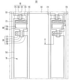
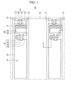
Organic light emitting diode (OLED) display
PatentActiveUS20110215302A1
Innovation
- The implementation of a translucent insulating layer filter on the encapsulation substrate, which forms a microcavity with the encapsulation substrate, reduces the need for fine metal masks by using separate patterned portions for each pixel and a continuous layer for all pixels, improving light efficiency and reducing mask usage.
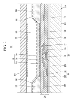
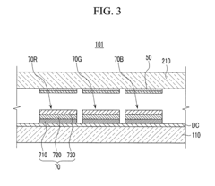
Encapsulated light emitting diodes for selective fluidic assembly
PatentActiveUS12119432B2
Innovation
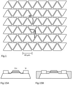
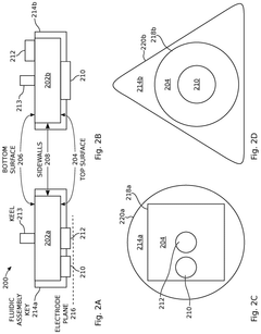
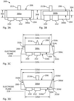
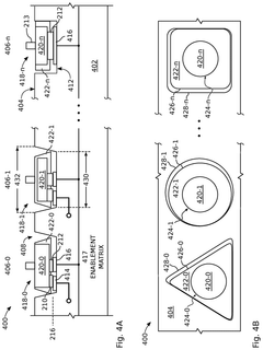
- The use of partially encapsulated semiconductor-based inorganic micro-LEDs with a patternable polymer encapsulant that protects the LEDs from collisions and optimizes their shape for efficient assembly, allowing for higher speed and yield while preventing defects, and enabling precise alignment of LED colors on a display substrate.
Energy Efficiency Comparison and Environmental Impact
The energy efficiency of display technologies is a critical factor in their commercial viability and environmental impact. OLED and MicroLED represent two distinct approaches to electromagnetic spectrum utilization, with significant implications for power consumption and sustainability.
OLED displays demonstrate superior energy efficiency when displaying darker content due to their emissive nature, where black pixels consume virtually no power. This characteristic makes OLEDs particularly efficient for applications with predominantly dark interfaces or content. However, when displaying bright or white content, OLEDs require more power as each pixel must actively emit light. Current OLED technology achieves approximately 20-40% energy conversion efficiency, with significant energy lost as heat during operation.
MicroLED technology, while still evolving, promises theoretical energy efficiency advantages over OLED. MicroLEDs can achieve higher brightness levels with lower power consumption, potentially reaching 30-50% energy conversion efficiency. This improved efficiency stems from better quantum yield and reduced internal reflection losses. The inorganic nature of MicroLEDs also allows for more efficient thermal management, reducing energy waste through heat dissipation.
From an environmental perspective, the manufacturing processes for these technologies present distinct challenges. OLED production typically involves organic solvents and potentially hazardous materials, raising concerns about waste management and disposal. The shorter lifespan of OLED displays (typically 30,000-60,000 hours before significant brightness degradation) also contributes to electronic waste generation.
MicroLED manufacturing currently requires more energy-intensive processes, including epitaxial growth and precision transfer techniques. However, the significantly longer theoretical lifespan of MicroLED displays (potentially exceeding 100,000 hours) could offset these initial environmental costs through reduced replacement frequency and associated electronic waste.
The carbon footprint comparison between these technologies must consider the entire lifecycle. While MicroLEDs may require more energy during production, their superior longevity and operational efficiency could result in a lower overall environmental impact. Recent lifecycle assessments suggest that a MicroLED display might reduce lifetime carbon emissions by 30-40% compared to equivalent OLED displays, primarily through extended service life and reduced power consumption during operation.
Water usage represents another environmental consideration, with OLED manufacturing typically requiring 20-30% more water than projected for optimized MicroLED production processes. As manufacturing techniques evolve, particularly for MicroLED, opportunities for further reducing environmental impact through improved resource utilization and recycling programs continue to emerge.
Supply Chain Considerations for Next-Generation Displays
The supply chain for next-generation display technologies like OLED and MicroLED represents a complex ecosystem with significant implications for market adoption and technological advancement. Both technologies require specialized materials and manufacturing processes that create distinct supply chain dynamics and challenges.
OLED supply chains are relatively mature, with established production facilities primarily concentrated in East Asia. Key materials include organic compounds, flexible substrates, and thin-film transistors. Samsung and LG Display dominate OLED panel production, creating potential bottlenecks and price volatility. The supply chain's concentration presents geopolitical vulnerabilities, as demonstrated during recent global disruptions.
MicroLED supply chains remain nascent and fragmented, presenting both challenges and opportunities. The technology requires ultra-precise manufacturing capabilities for transferring millions of microscopic LED chips to substrates. Current production methods are labor-intensive and expensive, limiting mass production feasibility. Key materials include semiconductor wafers, specialized phosphors, and advanced packaging materials.
The electromagnetic spectrum utilization differences between these technologies directly impact supply chain considerations. OLED's broader spectrum emission requires fewer specialized materials but demands precise organic compound formulation. MicroLED's narrower spectral output necessitates specific semiconductor materials optimized for different wavelengths, complicating material sourcing and quality control.
Equipment suppliers represent another critical supply chain component. OLED manufacturing relies on specialized deposition equipment from companies like Applied Materials and Canon Tokki, with the latter facing persistent order backlogs. MicroLED requires advanced pick-and-place machinery and inspection systems still under development by companies like ASM Pacific Technology and Kulicke & Soffa.
Sustainability considerations increasingly influence supply chain development. OLED production involves potentially hazardous organic compounds requiring careful handling and disposal. MicroLED manufacturing consumes significant energy but may offer longer-term sustainability benefits through extended device lifespans and reduced material consumption over time.
Looking forward, supply chain resilience will be crucial for both technologies. Diversification of manufacturing locations, vertical integration strategies, and development of alternative material sources will help mitigate risks. Companies investing in either technology must carefully evaluate supply chain maturity, regional dependencies, and potential disruption risks as part of their strategic planning process.
Unlock deeper insights with Patsnap Eureka Quick Research — get a full tech report to explore trends and direct your research. Try now!
Generate Your Research Report Instantly with AI Agent
Supercharge your innovation with Patsnap Eureka AI Agent Platform!