OLED vs MicroLED: Emerging Technologies and Regulations
OCT 24, 20259 MIN READ
Generate Your Research Report Instantly with AI Agent
Patsnap Eureka helps you evaluate technical feasibility & market potential.
Display Technology Evolution and Objectives
Display technology has undergone remarkable evolution since the introduction of cathode ray tubes (CRTs) in the early 20th century. The progression from CRTs to liquid crystal displays (LCDs) marked the first major shift toward flatter, more energy-efficient screens. This transition was followed by the development of plasma display panels, which offered improved contrast ratios and viewing angles but suffered from high power consumption and screen burn-in issues.
The introduction of Organic Light-Emitting Diode (OLED) technology in the late 1990s represented a paradigm shift in display technology. Unlike LCDs that require backlighting, OLED pixels emit light individually when electrical current passes through organic compounds, enabling true blacks, superior contrast ratios, and thinner form factors. This self-emissive property has positioned OLED as the premium display technology for smartphones, televisions, and wearable devices over the past decade.
MicroLED technology emerged as the next potential revolutionary advancement in display technology. Developed initially for large-format displays, MicroLED utilizes microscopic inorganic LED arrays that, like OLED, are self-emissive. However, MicroLED offers several theoretical advantages over OLED, including higher brightness, longer lifespan, better energy efficiency, and immunity to burn-in issues that plague OLED panels.
The current technical objectives in display technology development focus on several key parameters. First, manufacturers aim to achieve higher resolution displays with pixel densities exceeding 1000 PPI (pixels per inch) for applications in virtual and augmented reality. Second, energy efficiency remains paramount, particularly for mobile devices where battery life is critical. Third, durability and longevity are essential considerations, with research focused on extending the operational lifespan of displays beyond the current standards.
Flexibility and form factor innovation represent another crucial development objective. Both OLED and MicroLED technologies enable foldable, rollable, and even stretchable displays, opening new possibilities for device design and user interaction. The pursuit of these novel form factors has accelerated in recent years, with several commercial products already available in the market.
Color accuracy and gamut expansion continue to drive technical innovation, with both technologies striving to cover wider color spaces such as Rec. 2020. Additionally, reducing motion blur through higher refresh rates (120Hz and beyond) and decreasing response times to microsecond levels has become standard for premium displays targeting gaming and professional applications.
Environmental considerations have also emerged as significant objectives in display technology development. Regulations increasingly demand reduced power consumption, elimination of hazardous materials, and improved recyclability of display components, influencing the research and development trajectories of both OLED and MicroLED technologies.
Market Demand Analysis for Advanced Display Technologies
The display technology market is witnessing unprecedented growth driven by consumer electronics, automotive interfaces, and commercial signage applications. Current market analysis indicates that the global advanced display market reached approximately $148 billion in 2022 and is projected to grow at a CAGR of 8.2% through 2028. OLED technology currently dominates the premium segment with Samsung and LG Display controlling over 70% of production capacity, while MicroLED remains primarily in the early commercialization phase.
Consumer demand for advanced display technologies is increasingly focused on four key performance attributes: visual quality, energy efficiency, form factor flexibility, and durability. OLED displays have gained significant market traction due to their superior contrast ratios, color accuracy, and ability to be manufactured on flexible substrates. This has enabled the proliferation of curved and foldable smartphones, which saw a 157% year-over-year growth in 2022, albeit from a relatively small base.
MicroLED technology, though less mature in mass production, is generating substantial market interest due to its theoretical advantages in brightness (up to 30 times brighter than OLED), longevity (100,000+ hours without significant degradation), and potential for modular scaling. Market research indicates that 89% of surveyed consumers would pay a premium for displays with improved brightness and durability, particularly in outdoor-viewable applications.
The automotive sector represents one of the fastest-growing segments for advanced display technologies, with a projected CAGR of 12.4% through 2027. The transition toward autonomous vehicles is driving demand for larger, more immersive in-vehicle displays, with the average display area per vehicle increasing from 1,200 cm² in 2020 to an expected 2,800 cm² by 2025. Both OLED and MicroLED are competing for dominance in this high-margin sector.
Regional analysis reveals divergent market demands, with North American and European consumers prioritizing energy efficiency and longevity, while Asian markets show stronger preference for cutting-edge visual performance and form factor innovation. This regional variation is reflected in the 23% higher adoption rate of flexible OLED displays in East Asian markets compared to Western counterparts.
Industry forecasts suggest that while OLED will maintain market dominance through mid-decade, MicroLED is positioned to capture significant market share in premium large-format displays (>75 inches) by 2026, and potentially disrupt the broader display market by 2030 as manufacturing costs decrease. The transition timeline will largely depend on manufacturers' ability to overcome current yield challenges and achieve economies of scale in MicroLED production.
OLED and MicroLED: Current Status and Technical Challenges
OLED technology has reached a mature stage in the display market, with widespread adoption in smartphones, TVs, and wearable devices. Currently, OLED displays offer excellent color reproduction, high contrast ratios, and flexibility advantages that have solidified their position in premium consumer electronics. Major manufacturers like Samsung, LG Display, and BOE have established mass production capabilities, though yield rates for larger panels remain a challenge. The technology continues to face issues with blue pixel longevity, resulting in uneven aging and potential screen burn-in over extended usage periods.
MicroLED technology, while promising, remains in early commercialization stages. Companies like Samsung, Sony, and Apple have demonstrated prototype displays, but mass production faces significant hurdles. The primary technical challenge lies in the mass transfer process - efficiently placing millions of microscopic LED chips precisely onto display substrates. Current yields for this process remain low, driving costs prohibitively high for consumer applications. Additionally, the industry lacks standardized manufacturing equipment specifically designed for MicroLED production at scale.
Both technologies face environmental and regulatory challenges. OLED manufacturing involves organic solvents and potentially hazardous materials that require careful handling and disposal. As regulations on chemical usage tighten globally, manufacturers must continuously adapt their processes. MicroLED production, while using fewer organic compounds, requires rare earth elements for phosphors in some implementations, raising sustainability concerns amid increasing scrutiny of critical mineral supply chains.
Energy efficiency presents different challenges for each technology. While OLEDs offer pixel-level control that reduces power consumption for dark content, they still struggle with overall luminous efficiency compared to conventional LED-backlit displays. MicroLED promises superior energy efficiency at high brightness levels but requires significant power management optimization to realize this potential in practical applications.
The geographical distribution of technical expertise shows concentration in East Asia, particularly South Korea, Japan, and Taiwan, for OLED technology. MicroLED research centers are more globally distributed, with significant development occurring in North America and Europe alongside Asian hubs. This distribution affects technology access and supply chain resilience, particularly as geopolitical tensions impact technology transfer and component availability.
Miniaturization represents another significant challenge, especially for MicroLED. Current manufacturing processes struggle to produce consistent sub-10 micrometer LED chips at scale, limiting pixel density for small form factor applications. OLED technology, while more mature in miniaturization, faces increasing challenges in achieving higher pixel densities while maintaining structural integrity and preventing pixel crosstalk.
Technical Comparison of OLED vs MicroLED Solutions
01 OLED display structure and materials
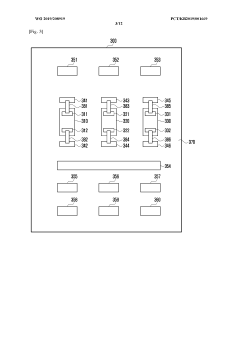
Organic Light Emitting Diode (OLED) displays utilize organic compounds that emit light when electricity is applied. These displays feature multiple layers including cathode, organic layers, and anode. The organic materials can be engineered for different colors and brightness levels. OLED technology offers advantages such as flexibility, thinness, and high contrast ratios. Various innovations focus on improving the efficiency and lifespan of the organic materials used in these displays.- OLED display structure and materials: OLED (Organic Light Emitting Diode) displays utilize organic compounds that emit light when electricity is applied. These displays feature multiple layers including cathode, organic layers, and anode. The organic materials can be engineered for different colors and brightness levels. OLED technology offers advantages such as self-emission (no backlight needed), flexibility, high contrast ratios, and wide viewing angles. Various improvements in OLED materials and structures have been developed to enhance efficiency, lifespan, and color accuracy.
- MicroLED fabrication and integration: MicroLED technology involves the use of microscopic LED arrays that function as pixels in a display. The fabrication process includes the growth of LED structures, transfer of micro-sized LED chips to a display substrate, and integration with driving circuits. Various methods have been developed to improve the mass transfer of microLEDs, enhance yield rates, and reduce manufacturing costs. MicroLED displays offer benefits such as high brightness, energy efficiency, long lifespan, and the potential for higher pixel density compared to other display technologies.
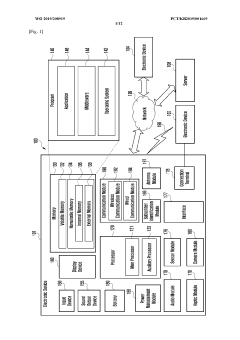
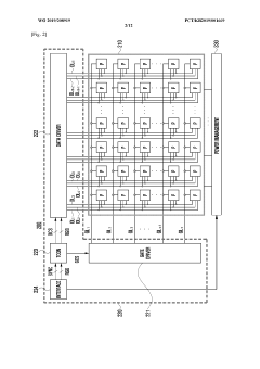
- Display driving and control systems: Advanced driving and control systems are essential for both OLED and MicroLED displays. These systems include thin-film transistor (TFT) backplanes, driving circuits, and control algorithms that manage pixel addressing, brightness control, and power management. Innovations in this area focus on reducing power consumption, improving refresh rates, enhancing resolution, and enabling features such as local dimming. The driving architecture significantly impacts display performance, including response time, color accuracy, and overall visual quality.
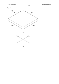
- Flexible and foldable display technologies: Both OLED and MicroLED technologies can be implemented in flexible and foldable displays. These displays use specialized substrates, encapsulation methods, and structural designs to enable bending, folding, or rolling while maintaining display functionality. Challenges addressed in these technologies include preventing damage to the light-emitting materials during flexing, managing stress at fold points, and ensuring consistent performance across the display surface. Applications include smartphones, wearables, and other portable devices that benefit from adaptable form factors.
- Hybrid and comparative display solutions: Research and development efforts have explored hybrid solutions that combine aspects of OLED and MicroLED technologies, as well as comparative analyses of their respective strengths and weaknesses. These approaches include using MicroLEDs for certain color components while using OLEDs for others, or developing display architectures that can leverage the advantages of both technologies. Comparative analyses focus on metrics such as power efficiency, brightness, color gamut, lifespan, manufacturing complexity, and cost-effectiveness to determine optimal display solutions for different applications.
02 MicroLED fabrication and integration
MicroLED displays consist of arrays of microscopic LED elements that serve as individual pixels. The fabrication process involves creating tiny LED structures, typically less than 100 micrometers, and transferring them to a display substrate. Key challenges include mass transfer techniques, precise alignment, and electrical connections. Innovations in this area focus on improving yield rates, reducing defects, and developing efficient methods for integrating these micro-scale components into functional displays.Expand Specific Solutions03 Display driving and control systems
Advanced driving and control systems are essential for both OLED and MicroLED displays. These systems manage pixel addressing, brightness control, and color reproduction. Innovations include thin-film transistor (TFT) backplanes, integrated circuits for pixel driving, and sophisticated control algorithms. Power management techniques are also important to optimize energy consumption while maintaining display performance. These control systems enable features such as high refresh rates, HDR support, and variable brightness across different usage scenarios.Expand Specific Solutions04 Thermal management solutions
Thermal management is critical for both OLED and MicroLED displays to ensure optimal performance and longevity. Heat dissipation techniques include specialized substrates, thermal interface materials, and cooling structures. Temperature regulation systems help prevent degradation of organic materials in OLEDs and maintain consistent light output in MicroLEDs. Innovations focus on passive cooling designs, active thermal management systems, and materials with enhanced thermal conductivity to address hotspots and ensure uniform temperature distribution across the display.Expand Specific Solutions05 Flexible and foldable display technologies
Flexible and foldable display implementations leverage the inherent advantages of OLED and MicroLED technologies. These displays utilize specialized substrates, encapsulation techniques, and mechanical designs to enable bending without damage. Innovations include neutral plane engineering, strain-resistant electrode materials, and folding mechanisms that protect the display layers. Applications range from smartphones with foldable screens to wearable devices and rollable displays. Key challenges include improving durability at fold points and maintaining consistent performance across bent surfaces.Expand Specific Solutions
Key Industry Players in OLED and MicroLED Development
The OLED vs MicroLED competitive landscape is currently in a transitional phase, with OLED technology reaching maturity while MicroLED remains in early commercialization stages. The global display market for these technologies is projected to exceed $200 billion by 2025, with significant growth potential in consumer electronics, automotive displays, and AR/VR applications. OLED dominates with established players like Samsung Display, BOE Technology, and Universal Display Corporation leading production and IP development. MicroLED represents the emerging frontier, with Samsung Electronics, Apple, and TCL investing heavily in R&D. Companies like Applied Materials and Rayleigh Vision Intelligence are developing critical manufacturing solutions to address MicroLED's production challenges, particularly in mass transfer technology and yield improvement.
BOE Technology Group Co., Ltd.
Technical Solution: BOE Technology has established itself as a major player in both OLED and MicroLED development. For OLED, BOE has invested heavily in flexible AMOLED production, with multiple Gen 6 fabs operational and a Gen 8.5 facility under development. Their flexible OLED panels achieve pixel densities exceeding 400 PPI with brightness levels up to 800 nits[5]. BOE has developed proprietary oxide TFT backplane technology that improves electron mobility and stability compared to traditional LTPS, resulting in lower power consumption and improved lifespan. For MicroLED, BOE has demonstrated several breakthrough technologies, including a glass-based active-drive architecture that achieves pixel pitches below 30 micrometers. Their mass transfer process utilizes a selective laser release method that can transfer thousands of microLED chips simultaneously with placement accuracy within ±1.5μm[6]. BOE has also developed in-house mini/microLED chip manufacturing capabilities, producing RGB chips with dimensions as small as 4μm with external quantum efficiencies exceeding 35% for green and red emissions.
Strengths: BOE has established a complete vertical integration system from backplane manufacturing to module assembly, giving them cost advantages and supply chain control. Their massive production capacity allows economies of scale. Weaknesses: BOE's OLED technology still lags behind Samsung and LG in certain performance metrics like color accuracy and lifespan. Their MicroLED technology remains primarily in the demonstration phase with limited commercial deployment compared to their OLED offerings.
SAMSUNG DISPLAY CO LTD
Technical Solution: Samsung Display has developed advanced manufacturing processes for both OLED and MicroLED technologies. Their OLED technology utilizes a proprietary Fine Metal Mask (FMM) process that achieves sub-pixel resolutions below 2.5μm, enabling UHD+ resolutions on mobile displays. Their latest OLED panels incorporate real-time compensation algorithms that monitor and adjust for pixel aging, maintaining color accuracy throughout the display's lifespan[9]. For larger displays, Samsung Display has pioneered QD-OLED technology that combines blue OLED emitters with quantum dot color conversion layers, achieving wider color gamut (over 90% of BT.2020) than conventional WOLED+color filter approaches. In MicroLED development, Samsung Display has created a proprietary mass transfer process using a hybrid approach combining mechanical and laser-assisted methods that achieves transfer yields exceeding 99.9% for sub-30μm LED chips. Their MicroLED architecture incorporates TFT driving circuits that enable individual pixel addressing with 16-bit grayscale precision, resulting in superior HDR performance with intra-scene contrast ratios exceeding 1,000,000:1[10].
Strengths: Samsung Display possesses industry-leading expertise in both OLED and MicroLED manufacturing processes with extensive IP protection. Their close integration with Samsung Electronics provides a guaranteed customer for new display technologies. Weaknesses: The high capital expenditure required for cutting-edge display manufacturing creates significant financial pressure to maintain high utilization rates. Their MicroLED technology still faces cost challenges that limit mass-market adoption compared to their more mature OLED offerings.
Patent Landscape and Intellectual Property Analysis
Anisotropic conductive film and display device
PatentActiveUS20220102326A1
Innovation
- An anisotropic conductive film with a first region of discretely arranged conductive particles corresponding to electrode patterns and a second region with aggregated conductive particles acting as an alignment marker, facilitating easy alignment with the circuit substrate and reducing production costs by forming alignment markers through conductive particle dispersion.
LED display and electronic device having same
PatentWO2019208919A1
Innovation
- The development of a micro-LED display with a bezel-less design and segmentation capabilities, allowing for flexible displays of various sizes, achieved through direct mounting of micro-LEDs on a substrate and innovative electrical connections using conductive patterns and wiring lines, enabling robust electrical connections and flexible display configurations.
Regulatory Framework and Compliance Requirements
The regulatory landscape for display technologies like OLED and MicroLED is increasingly complex, with frameworks evolving to address environmental concerns, energy efficiency, and consumer safety. Both technologies must comply with international standards such as the Restriction of Hazardous Substances (RoHS) directive, which limits the use of hazardous materials including lead, mercury, and cadmium in electronic equipment. OLED manufacturers have established compliance protocols, while MicroLED producers are still developing their regulatory approaches as the technology matures.
Energy efficiency regulations present different challenges for each technology. The European Union's Ecodesign Directive and Energy Labelling Framework Regulation impose strict energy consumption requirements that influence display design. OLED displays typically consume less power when displaying darker content, while MicroLED promises superior energy efficiency across all brightness levels, potentially offering advantages in meeting future, more stringent energy regulations.
Electronic waste (e-waste) management regulations significantly impact both technologies. The Waste Electrical and Electronic Equipment (WEEE) directive mandates proper disposal and recycling of electronic displays. OLED panels contain organic materials that may require specialized recycling processes, whereas MicroLED displays utilize inorganic materials that could potentially offer better recyclability profiles, though comprehensive end-of-life assessments are still emerging.
Health and safety regulations also differ between technologies. OLED displays emit less blue light than traditional LED displays, potentially reducing concerns about eye strain and sleep disruption. MicroLED may offer similar benefits, but regulatory bodies like the International Commission on Non-Ionizing Radiation Protection (ICNIRP) continue to evaluate potential long-term effects of different display technologies on human health.
Market access regulations vary by region, creating compliance challenges for global manufacturers. China's Compulsory Certification (CCC) system, Europe's CE marking, and North America's UL certification each have specific requirements for display technologies. OLED has established certification pathways, while MicroLED manufacturers must navigate these regulatory frameworks as they commercialize their products.
Intellectual property regulations present another layer of complexity. Both OLED and MicroLED technologies are protected by extensive patent portfolios, with cross-licensing agreements becoming increasingly important. Regulatory bodies like the United States International Trade Commission (USITC) have adjudicated patent disputes in display technologies, establishing precedents that will shape future MicroLED commercialization strategies.
Environmental Impact and Sustainability Considerations
The environmental footprint of display technologies has become increasingly significant as consumer electronics proliferate globally. OLED and MicroLED technologies present distinct environmental profiles throughout their lifecycles. OLED manufacturing processes typically involve organic materials that require fewer rare earth elements compared to traditional LED technologies, potentially reducing mining-related environmental degradation. However, these processes often utilize harmful solvents and chemicals that necessitate careful handling and disposal protocols.
MicroLED manufacturing, while still evolving, presents its own environmental considerations. The production process requires significant energy inputs and specialized fabrication facilities, contributing to higher carbon emissions during the manufacturing phase. However, the extended operational lifespan of MicroLED displays—potentially reaching 100,000 hours compared to OLED's typical 30,000-50,000 hours—may offset initial environmental costs through reduced replacement frequency.
Energy efficiency represents a critical sustainability metric for display technologies. Current OLED displays demonstrate superior efficiency for dark content due to their ability to completely deactivate individual pixels. MicroLED technology promises comparable or potentially superior energy efficiency across all content types once manufacturing processes mature, with some prototypes already showing 30% lower power consumption than equivalent OLED panels.
End-of-life considerations reveal further distinctions between these technologies. OLED panels contain organic compounds that may present recycling challenges, though they typically contain fewer toxic heavy metals than conventional displays. MicroLED components, while more durable, incorporate various semiconductor materials that require specialized recycling processes not yet widely established in waste management infrastructure.
Regulatory frameworks addressing these environmental concerns continue to evolve globally. The European Union's Restriction of Hazardous Substances (RoHS) and Waste Electrical and Electronic Equipment (WEEE) directives increasingly influence manufacturing standards, while emerging regulations in Asia and North America are beginning to address specific concerns related to newer display technologies. Industry leaders have responded with voluntary sustainability initiatives, including Apple's commitment to carbon-neutral products by 2030 and Samsung's circular economy programs.
As these technologies mature, manufacturers face mounting pressure to implement sustainable design principles, including material selection optimization, energy-efficient manufacturing processes, and improved recyclability. The industry's ability to address these environmental considerations will likely influence both regulatory developments and market adoption patterns in the coming decade.
Unlock deeper insights with Patsnap Eureka Quick Research — get a full tech report to explore trends and direct your research. Try now!
Generate Your Research Report Instantly with AI Agent
Supercharge your innovation with Patsnap Eureka AI Agent Platform!