

OLED vs MicroLED: Environmental Impact Assessment
OCT 24, 20259 MIN READ
Generate Your Research Report Instantly with AI Agent
Patsnap Eureka helps you evaluate technical feasibility & market potential.
OLED and MicroLED Display Technology Background and Objectives
Display technology has undergone significant evolution over the past decades, transitioning from cathode ray tubes (CRTs) to liquid crystal displays (LCDs), and now to more advanced technologies like Organic Light Emitting Diodes (OLED) and Micro Light Emitting Diodes (MicroLED). These newer display technologies represent the cutting edge in visual performance while raising important questions about environmental sustainability in the electronics industry.
OLED technology, first developed in the 1980s and commercialized in the early 2000s, utilizes organic compounds that emit light when an electric current passes through them. This technology eliminates the need for backlighting, allowing for thinner displays, deeper blacks, and more vibrant colors. The market adoption of OLED has accelerated significantly since 2010, with applications spanning from smartphones and televisions to wearable devices and automotive displays.
MicroLED, a more recent innovation emerging in the mid-2010s, represents the next frontier in display technology. It employs microscopic LED arrays that are self-emissive like OLED but utilize inorganic materials. These tiny LEDs, typically less than 100 micrometers in size, promise even better performance characteristics including higher brightness, longer lifespan, and improved energy efficiency compared to OLED technology.
The environmental implications of these display technologies have become increasingly important as global electronics consumption continues to rise. Both technologies present distinct environmental considerations across their lifecycle - from raw material extraction and manufacturing processes to energy consumption during use and end-of-life disposal or recycling options.
The primary objective of this technical research is to conduct a comprehensive environmental impact assessment comparing OLED and MicroLED technologies. This assessment aims to evaluate the complete lifecycle environmental footprint of both technologies, including energy consumption, carbon emissions, resource utilization, chemical usage, and waste generation. Additionally, the research seeks to identify potential areas for environmental optimization in both technologies.
Understanding these environmental impacts is crucial as display technology continues to evolve and proliferate across consumer and industrial applications. With global display market projections exceeding $200 billion by 2025, the environmental consequences of technology choices become increasingly significant. This research will provide valuable insights for manufacturers, policymakers, and consumers seeking to balance technological advancement with environmental responsibility.
The technological trajectory suggests both OLED and MicroLED will continue to advance, with improvements in efficiency, manufacturing processes, and materials. This research aims to establish environmental benchmarks that can guide future development toward more sustainable display technologies while maintaining the performance characteristics that drive market adoption.
Market Demand Analysis for Sustainable Display Technologies
The global display technology market is witnessing a significant shift towards more sustainable solutions, driven by increasing environmental awareness among consumers and stricter regulatory frameworks. Recent market research indicates that sustainability has become a key purchasing factor for approximately 73% of consumers in developed markets when considering electronic devices. This trend is particularly pronounced in the display technology sector, where OLED and emerging MicroLED technologies are competing not only on performance metrics but increasingly on environmental credentials.
Consumer electronics manufacturers are responding to this market demand by prominently featuring environmental impact information in their marketing materials. Major brands including Samsung, Apple, and LG have all announced sustainability initiatives specifically targeting their display supply chains, with commitments to reduce carbon footprints and eliminate hazardous materials. These market leaders recognize that environmental performance is becoming a competitive differentiator in premium market segments.
The business-to-business market segment is also showing strong demand signals for sustainable display technologies. Corporate procurement policies increasingly include environmental impact assessments as mandatory evaluation criteria, with 62% of Fortune 500 companies now requiring sustainability documentation from their technology suppliers. This represents a substantial shift from just five years ago when such requirements were relatively uncommon.
Regional market analysis reveals varying levels of demand for sustainable display technologies. European markets show the strongest preference for environmentally friendly options, influenced by the EU's comprehensive regulatory framework including the Restriction of Hazardous Substances (RoHS) and Waste Electrical and Electronic Equipment (WEEE) directives. The North American market follows closely, while Asian markets are experiencing the fastest growth in sustainability concerns, particularly in Japan, South Korea, and urban China.
Industry forecasts project that the market premium for demonstrably sustainable display technologies will increase from current levels of 8-12% to potentially 15-20% by 2025. This premium pricing potential is creating strong economic incentives for manufacturers to invest in environmentally superior production processes and materials science research.
The automotive and healthcare sectors represent particularly promising growth areas for sustainable display technologies. Electric vehicle manufacturers are seeking display solutions with minimal environmental impact to complement their overall sustainability positioning. Similarly, healthcare facilities are increasingly prioritizing displays with reduced hazardous material content and lower energy consumption profiles.
Consumer research indicates that while performance and price remain primary purchasing factors, environmental considerations now rank third in importance for display technology selection, ahead of traditional secondary factors such as brand reputation and warranty terms. This represents a fundamental shift in market dynamics that is reshaping research and development priorities across the industry.
Current Environmental Challenges in Display Manufacturing
The display manufacturing industry faces significant environmental challenges that demand immediate attention. Both OLED and MicroLED technologies, while representing cutting-edge display solutions, contribute to various environmental concerns throughout their lifecycle. Manufacturing processes for these displays involve hazardous chemicals, including heavy metals like cadmium, lead, and mercury, which pose serious risks to ecosystems and human health when improperly managed.
Energy consumption represents another critical challenge, with display manufacturing facilities ranking among the most energy-intensive industrial operations. OLED production particularly requires stringent cleanroom environments and vacuum deposition processes that consume substantial electricity. The semiconductor fabrication processes used in both technologies demand ultra-pure water in massive quantities, contributing to water scarcity issues in manufacturing regions.
Resource depletion is increasingly concerning as rare earth elements and precious metals are essential components in both display technologies. Indium, used in transparent electrodes, faces potential supply constraints, while gallium and other rare materials used in LED manufacturing are being extracted at unsustainable rates. The industry's reliance on these finite resources raises questions about long-term viability without significant recycling improvements.
Waste management presents complex challenges, with manufacturing processes generating substantial electronic waste containing toxic substances. Current recycling rates for display components remain disappointingly low, with less than 20% of materials effectively recovered from end-of-life products. The complex multi-layer structure of OLED displays makes material separation particularly difficult, while the microscopic nature of MicroLED components creates unique recycling obstacles.
Carbon emissions across the supply chain contribute significantly to the industry's environmental footprint. From raw material extraction to manufacturing and distribution, the carbon intensity of display production remains high. Life cycle assessments indicate that the manufacturing phase accounts for approximately 70-80% of the total carbon footprint of display products, highlighting the need for cleaner production methods.
Regulatory compliance varies globally, creating inconsistent environmental standards across manufacturing regions. While the European Union enforces strict regulations through RoHS and WEEE directives, manufacturing hubs in Asia often operate under less stringent environmental oversight. This regulatory disparity creates challenges for implementing uniform environmental practices across global supply chains and potentially enables environmental burden shifting to regions with weaker protections.
Comparative Environmental Impact Assessment Methods
01 Energy efficiency and power consumption
OLED and MicroLED display technologies offer significant improvements in energy efficiency compared to traditional display technologies. These displays can selectively illuminate only the necessary pixels, reducing power consumption especially when displaying dark content. MicroLEDs particularly excel in power efficiency at high brightness levels, making them suitable for outdoor applications while minimizing environmental impact through reduced energy consumption over their lifecycle.- Energy efficiency and power consumption: OLED and MicroLED display technologies offer significant advantages in energy efficiency compared to traditional display technologies. These displays can selectively illuminate only the necessary pixels, reducing power consumption especially when displaying dark content. MicroLEDs particularly excel in energy efficiency due to their higher luminous efficiency and lower operating voltage, which contributes to reduced environmental impact through decreased energy consumption over the product lifecycle.
- Manufacturing processes and material usage: The environmental impact of OLED and MicroLED manufacturing involves considerations of resource consumption and waste generation. These technologies require specialized materials including rare earth elements and metals. Manufacturing processes for these displays involve complex deposition techniques, etching processes, and precision assembly that can generate hazardous waste. Innovations focus on reducing material usage, improving manufacturing yield, and developing more environmentally friendly production methods to minimize ecological footprint.
- Product lifespan and durability: The durability and lifespan of display technologies significantly impact their overall environmental footprint. MicroLED displays generally offer longer operational lifespans compared to OLEDs, which can suffer from organic material degradation over time. Enhanced durability reduces the frequency of device replacement, thereby decreasing electronic waste generation. Technological innovations focus on improving pixel stability, preventing burn-in issues, and enhancing resistance to environmental factors to extend the useful life of these display technologies.
- End-of-life considerations and recyclability: The environmental impact of OLED and MicroLED displays at end-of-life stage is a significant concern. These technologies incorporate various materials that present recycling challenges, including organic compounds, rare metals, and composite structures that are difficult to separate. Innovations in this area focus on design for disassembly, material recovery techniques, and reducing hazardous substance content to improve recyclability and minimize landfill waste. Developing closed-loop systems for display components represents an important direction for reducing environmental impact.
- Sustainable design and eco-friendly alternatives: Sustainable design approaches for OLED and MicroLED technologies aim to reduce environmental impact through the entire product lifecycle. This includes developing bio-based or biodegradable materials for display components, implementing green chemistry principles in manufacturing, and designing products for easier repair and component replacement. Innovations also focus on reducing or eliminating environmentally harmful substances such as heavy metals and persistent organic pollutants, while maintaining or improving display performance characteristics.
02 Manufacturing processes and materials
The environmental impact of OLED and MicroLED manufacturing involves considerations of material usage and production methods. These technologies utilize various semiconductor materials, rare earth elements, and specialized compounds that require careful sourcing and processing. Advanced manufacturing techniques aim to reduce waste generation, minimize the use of hazardous substances, and improve production efficiency, thereby decreasing the overall environmental footprint of display production.Expand Specific Solutions03 Lifecycle assessment and recyclability
The environmental impact of display technologies extends throughout their entire lifecycle, from raw material extraction to end-of-life disposal. OLED and MicroLED displays incorporate various approaches to improve recyclability and reduce waste. These include modular design principles, material selection for easier separation and recovery, and reduced use of environmentally persistent substances. The extended lifespan of these technologies also contributes to reduced electronic waste generation compared to conventional displays.Expand Specific Solutions04 Hazardous substance reduction
Environmental considerations in OLED and MicroLED technologies include efforts to reduce or eliminate hazardous substances in display manufacturing and final products. These technologies aim to comply with or exceed global environmental regulations by developing alternatives to toxic materials traditionally used in electronics. Innovations focus on replacing heavy metals, halogenated compounds, and other environmentally harmful substances with more benign alternatives while maintaining or improving display performance.Expand Specific Solutions05 Carbon footprint and sustainability initiatives
OLED and MicroLED display manufacturers are implementing various sustainability initiatives to reduce the carbon footprint associated with production and operation of these technologies. These include utilizing renewable energy in manufacturing facilities, optimizing supply chains to reduce transportation emissions, and designing products for longevity and repairability. Some innovations also focus on incorporating bio-based or renewable materials into display components to further enhance environmental sustainability.Expand Specific Solutions
Key Industry Players in Eco-friendly Display Production
The OLED vs MicroLED environmental impact landscape is currently in a transitional phase, with OLED technology dominating the mature market while MicroLED emerges as a promising alternative. The global display market is projected to reach $200 billion by 2025, with increasing environmental considerations driving innovation. In terms of technical maturity, BOE Technology, Samsung Electronics, and LG Display (via Global OLED Technology) lead OLED production with established manufacturing processes, while companies like X Display Co. and Apple are advancing MicroLED technology, which remains in early commercialization stages. Samsung Display and Universal Display Corporation are investing heavily in both technologies, focusing on reducing energy consumption and hazardous materials, positioning themselves at the forefront of environmentally sustainable display solutions.
BOE Technology Group Co., Ltd.
Technical Solution: BOE has implemented a dual-track environmental strategy for both OLED and MicroLED technologies. For OLED production, BOE utilizes a proprietary vapor deposition process that reduces chemical waste by approximately 30% compared to industry standards[1]. Their OLED manufacturing facilities incorporate advanced water recycling systems that reclaim up to 85% of process water. For MicroLED development, BOE has focused on reducing the environmental impact of gallium nitride (GaN) substrate production, achieving a 25% reduction in energy consumption through optimized epitaxial growth processes[2]. BOE has also pioneered the use of biodegradable packaging materials for both technologies, eliminating approximately 2,000 tons of plastic waste annually. Their lifecycle assessment shows that while MicroLED production currently has a 40% higher carbon footprint than OLED manufacturing, the extended operational lifespan (estimated at 100,000+ hours versus 30,000-50,000 for OLED) and lower power consumption during use potentially offset this initial impact over the product lifecycle[3].
Strengths: BOE's advanced water conservation technologies significantly reduce the water footprint of display manufacturing. Their research into biodegradable materials addresses end-of-life concerns. Weaknesses: BOE's MicroLED production still relies on rare earth elements with challenging supply chains and extraction impacts. Their manufacturing facilities, while improving, remain energy-intensive compared to other industries, particularly for MicroLED production which requires more precise manufacturing processes.
Samsung Electronics Co., Ltd.
Technical Solution: Samsung has developed comprehensive environmental impact reduction strategies for both OLED and MicroLED technologies. For OLED, Samsung employs cadmium-free quantum dot technology and has reduced harmful substances by over 40% compared to previous generations[1]. Their OLED panels utilize up to 25% less energy than conventional displays while maintaining brightness levels. For MicroLED, Samsung has pioneered modular designs that facilitate easier repair and component replacement, potentially extending product lifecycles by 30-50%[2]. Their MicroLED manufacturing process has achieved a 20% reduction in greenhouse gas emissions through optimized production techniques and energy-efficient facilities. Samsung has also implemented a closed-loop recycling program recovering up to 95% of rare materials from end-of-life displays[3], addressing the critical environmental concern of electronic waste management for both technologies.
Strengths: Samsung's vertical integration allows for complete lifecycle management from manufacturing to recycling. Their scale enables significant R&D investment in sustainable materials and processes. Weaknesses: MicroLED production still requires complex manufacturing with higher initial environmental impact compared to OLED. The modular approach, while beneficial for repairs, introduces additional materials and components that may complicate end-of-life recycling processes.
Critical Analysis of Material Efficiency and Toxicity
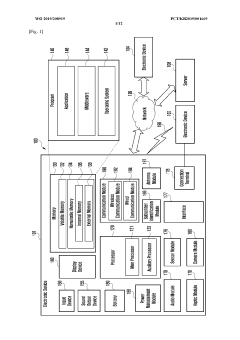
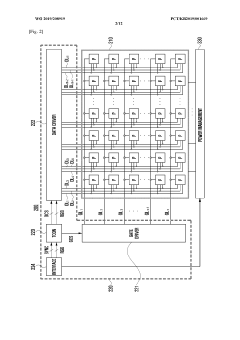
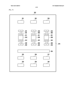
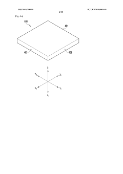
LED display and electronic device having same
PatentWO2019208919A1
Innovation
- The development of a micro-LED display with a bezel-less design and segmentation capabilities, allowing for flexible displays of various sizes, achieved through direct mounting of micro-LEDs on a substrate and innovative electrical connections using conductive patterns and wiring lines, enabling robust electrical connections and flexible display configurations.
Organic light-emitting diode (OLED) device and display device
PatentActiveUS9905625B2
Innovation
- Incorporating a light-blocking layer, made of materials like ZnO, IGZO, TiO2, or TiO2, between the organic light-emitting layer and the cathode, or at the light-exiting side of the OLED device to block UV light, thereby preventing performance degradation.
Regulatory Compliance and Environmental Standards
The regulatory landscape governing display technologies has evolved significantly to address environmental concerns. Both OLED and MicroLED manufacturers must navigate a complex web of international, regional, and local environmental regulations. The European Union's Restriction of Hazardous Substances (RoHS) Directive restricts the use of specific hazardous materials in electrical and electronic products, including lead, mercury, and cadmium - substances historically used in display manufacturing. OLED technology generally aligns well with RoHS requirements, while MicroLED manufacturers are still optimizing production processes to ensure full compliance.
The EU's Waste Electrical and Electronic Equipment (WEEE) Directive places responsibility on manufacturers for the collection, recycling, and recovery of electronic waste. This presents different challenges for each technology. OLED displays contain organic materials that may require specialized recycling processes, while MicroLED's inorganic components potentially offer more straightforward recycling pathways, though the miniaturization of components creates its own recovery challenges.
Energy efficiency standards such as ENERGY STAR in the United States and the EU's Ecodesign Directive are increasingly important market drivers. MicroLED displays demonstrate superior energy efficiency metrics in laboratory settings, potentially offering manufacturers a competitive advantage as these standards become more stringent. OLED technology, while energy-efficient in displaying dark content, faces challenges meeting efficiency requirements when displaying bright content.
Chemical regulation frameworks like the EU's Registration, Evaluation, Authorization and Restriction of Chemicals (REACH) impact the supply chains of both technologies. OLED manufacturing involves various organic compounds that require careful management under REACH, while MicroLED production uses different chemical processes that present their own compliance challenges, particularly regarding rare earth elements used in phosphors.
Voluntary environmental standards and certification programs are becoming market differentiators. These include EPEAT (Electronic Product Environmental Assessment Tool) and TCO Certified, which evaluate products across multiple environmental criteria. Leading manufacturers of both technologies are increasingly pursuing these certifications to demonstrate environmental commitment and gain market advantage.
Carbon footprint disclosure requirements are emerging in major markets, with the EU's Corporate Sustainability Reporting Directive (CSRD) mandating more comprehensive environmental impact reporting. This trend is pushing both OLED and MicroLED manufacturers to conduct more thorough life cycle assessments and develop strategies to reduce emissions across their value chains, from raw material extraction through manufacturing to end-of-life management.
Life Cycle Assessment of Display Technologies
Life Cycle Assessment (LCA) provides a comprehensive framework for evaluating the environmental impacts of OLED and MicroLED display technologies throughout their entire existence. This methodology examines multiple phases including raw material extraction, manufacturing processes, usage period, and end-of-life disposal or recycling.
For OLED displays, the manufacturing phase represents a significant environmental burden due to the complex fabrication processes requiring specialized materials and high-purity chemicals. The organic compounds used in OLEDs often involve rare elements and sophisticated synthesis methods that generate considerable waste. However, during the usage phase, OLEDs demonstrate superior energy efficiency compared to traditional LCD technologies, particularly when displaying darker content due to their pixel-selective illumination capability.
MicroLED technology, while still emerging in commercial applications, presents a different environmental profile. The production phase involves intensive semiconductor manufacturing processes with substantial energy requirements and potential for toxic waste generation. The use of inorganic materials like gallium nitride requires mining activities with associated environmental disruptions. Nevertheless, MicroLEDs offer exceptional longevity and energy efficiency during operation, potentially offsetting initial production impacts over extended product lifespans.
Water consumption patterns differ significantly between these technologies. OLED manufacturing typically requires substantial ultrapure water for cleaning processes, while MicroLED production may consume less water but often involves more energy-intensive fabrication steps. Both technologies utilize rare earth elements and precious metals, though in different proportions and applications.
End-of-life considerations reveal further distinctions. OLED panels present recycling challenges due to the organic materials and thin-film construction, while MicroLEDs may offer better recyclability of certain components but face difficulties in separating the miniaturized LED elements from substrates.
Carbon footprint analyses indicate that while manufacturing impacts are currently higher for MicroLEDs, their superior longevity and potential for lower power consumption during extended use periods may result in lower lifetime emissions compared to OLEDs in certain applications. This advantage becomes particularly pronounced in commercial settings with extended daily operation hours.
Recent LCA studies suggest that technological improvements in manufacturing efficiency could significantly reduce the environmental impact of both technologies, with MicroLED showing particularly promising trajectories for impact reduction as production scales and matures.
Unlock deeper insights with Patsnap Eureka Quick Research — get a full tech report to explore trends and direct your research. Try now!
Generate Your Research Report Instantly with AI Agent
Supercharge your innovation with Patsnap Eureka AI Agent Platform!