OLED vs MicroLED: Impacts on Image Processing Technologies
OCT 24, 20259 MIN READ
Generate Your Research Report Instantly with AI Agent
PatSnap Eureka helps you evaluate technical feasibility & market potential.
OLED and MicroLED Evolution and Objectives
Display technology has undergone significant evolution since the introduction of cathode ray tubes (CRTs) in the early 20th century. The transition from CRTs to liquid crystal displays (LCDs) marked the first major shift toward flatter, more energy-efficient screens. OLED (Organic Light-Emitting Diode) technology emerged in the late 1980s, with the first practical OLED device developed by Eastman Kodak in 1987. This technology represented a paradigm shift by eliminating the need for backlighting, allowing for thinner displays with superior contrast ratios and power efficiency.
The commercial adoption of OLED displays accelerated in the 2010s, particularly in smartphones and premium televisions. Samsung and LG became early leaders, investing heavily in OLED manufacturing capabilities. The technology's ability to produce perfect blacks and wide color gamuts made it particularly attractive for high-end consumer electronics. However, challenges including limited brightness, burn-in issues, and high production costs have constrained its broader adoption in certain market segments.
MicroLED technology represents the next evolutionary step in display technology, conceptualized in the early 2000s but only recently approaching commercial viability. Unlike OLEDs, which use organic compounds, MicroLEDs utilize inorganic gallium nitride-based materials to create self-emissive pixels at microscopic scales (typically less than 100 micrometers). This fundamental difference addresses several limitations of OLED technology, including brightness capabilities, lifespan, and burn-in susceptibility.
The technical objectives for both technologies have evolved significantly. For OLED, current development focuses on improving luminous efficiency, extending operational lifespan, enhancing peak brightness, and reducing production costs through innovations in materials science and manufacturing processes. Particular emphasis is placed on blue OLED emitters, which historically have shorter lifespans than red and green counterparts.
For MicroLED, the primary objectives center on overcoming mass production challenges, particularly the complex and precise transfer process required to place millions of microscopic LEDs onto substrates. Reducing defect rates, improving yield, and developing cost-effective manufacturing techniques represent critical hurdles. Additionally, miniaturization efforts continue to push pixel sizes smaller while maintaining brightness and efficiency.
Both technologies are converging toward similar end-user objectives: achieving perfect black levels, wide color gamuts exceeding 100% DCI-P3, high dynamic range capabilities with peak brightness exceeding 1,000 nits, reduced power consumption, and form factor flexibility including transparency and foldability. The technical evolution trajectory suggests a future where display technologies will increasingly blur the boundaries between physical and digital environments, enabling new applications beyond traditional screens.
Market Demand Analysis for Advanced Display Technologies
The display technology market is witnessing unprecedented growth driven by increasing consumer demand for superior visual experiences across multiple devices. Current market analysis indicates that the global advanced display market is projected to reach $167 billion by 2025, with OLED technology currently dominating premium segments while MicroLED emerges as a promising contender. This growth trajectory is supported by expanding applications in smartphones, televisions, wearables, automotive displays, and commercial signage.
Consumer preferences are increasingly favoring displays with higher resolution, better color accuracy, improved brightness, and energy efficiency. OLED technology has established strong market penetration due to its perfect blacks, wide color gamut, and flexibility advantages. However, research indicates that 78% of high-end consumers express interest in MicroLED benefits once educated about its superior brightness and longevity characteristics.
The automotive sector represents a particularly fast-growing segment for advanced display technologies, with a compound annual growth rate of 19.3%. Vehicle manufacturers are integrating larger, more sophisticated displays that require advanced image processing capabilities to maintain clarity and responsiveness in variable lighting conditions. Both OLED and MicroLED technologies are competing intensely in this space, with each requiring distinct image processing approaches.
Commercial and professional markets demonstrate increasing demand for large-format displays with exceptional color accuracy and brightness. This segment values the burn-in resistance of MicroLED technology, with 63% of professional users citing image retention as a significant concern with current OLED implementations. The gaming industry similarly drives demand for displays with faster response times and higher refresh rates, creating specialized market niches where image processing technologies must evolve to eliminate motion blur and artifacts.
Regional analysis reveals that Asia-Pacific leads in advanced display technology adoption, accounting for 46% of global market share, followed by North America at 28% and Europe at 22%. Chinese manufacturers are rapidly expanding production capacity for both technologies, while Korean firms maintain leadership in OLED manufacturing expertise.
The transition between display technologies is creating significant demand for adaptive image processing solutions that can optimize content for the specific characteristics of each display type. Market research indicates that 84% of device manufacturers are investing in specialized image processing capabilities to differentiate their products, with particular emphasis on AI-enhanced algorithms that can dynamically adjust content rendering based on display technology and viewing conditions.
Current Technical Challenges in OLED and MicroLED
Despite significant advancements in both OLED and MicroLED technologies, several critical technical challenges persist that impact their performance and widespread adoption in display applications. For OLED displays, material degradation remains a fundamental issue, with blue OLED materials exhibiting shorter lifespans compared to red and green counterparts. This differential aging leads to color shift over time, requiring sophisticated compensation algorithms in image processing pipelines.
Burn-in effects continue to plague OLED displays, particularly in static interface elements, necessitating pixel shifting techniques and advanced wear leveling algorithms. These solutions increase computational requirements and add complexity to display drivers. Additionally, OLED's organic nature makes it susceptible to moisture and oxygen, requiring hermetic sealing that complicates manufacturing processes and increases production costs.
MicroLED technology faces its own set of challenges, primarily centered around mass transfer processes. The precise placement of millions of microscopic LED chips onto display substrates with near-perfect yield remains technically demanding. Current defect rates necessitate redundancy strategies and real-time defect compensation algorithms that must be integrated into image processing workflows.
Color uniformity presents another significant hurdle for MicroLED displays. Variations in LED chip characteristics require pixel-by-pixel calibration and compensation, substantially increasing the complexity of display drivers and processing requirements. The miniaturization of LED chips also creates thermal management challenges, as heat dissipation becomes more difficult at microscopic scales.
Both technologies struggle with power efficiency at different brightness levels. OLED displays exhibit non-linear power consumption curves that complicate power management, while MicroLED displays require sophisticated pulse width modulation techniques to achieve low brightness levels without introducing visible flicker.
From an image processing perspective, both technologies demand different approaches to handle their unique characteristics. OLED requires compensation for non-uniform pixel aging and prevention of static image retention, while MicroLED needs precise calibration for each individual emitter and defect management strategies. These requirements significantly impact the complexity of image processing pipelines and increase computational demands.
Manufacturing scalability remains problematic for both technologies but in different ways. OLED faces challenges in achieving consistent quality in large panels, while MicroLED struggles with transfer yield rates and assembly precision at scale. These manufacturing limitations directly influence production costs and market adoption rates.
Image Processing Solutions for OLED and MicroLED
01 Image processing techniques for OLED displays
Various image processing techniques are employed to enhance the visual quality of OLED displays. These include color calibration, brightness adjustment, and contrast enhancement algorithms specifically designed for OLED technology. These techniques compensate for the unique characteristics of OLED panels, such as their high contrast ratios and potential for burn-in, ensuring optimal image quality and extended display life.- Image processing techniques for OLED displays: Various image processing techniques are employed to enhance the visual quality of OLED displays. These include color calibration, brightness adjustment, and contrast enhancement algorithms specifically designed for OLED technology. These techniques compensate for the unique characteristics of OLED panels, such as their high contrast ratios and potential for burn-in, ensuring optimal image quality and extended display life.
- MicroLED display driving and control systems: MicroLED displays require specialized driving and control systems to manage their high pixel density and brightness capabilities. These systems include advanced pixel addressing schemes, current control mechanisms, and timing controllers that enable precise control of individual LED elements. Such technologies allow for improved power efficiency, faster response times, and enhanced image quality in MicroLED displays.
- Integration of image processing hardware with display technologies: Hardware solutions for integrating image processing capabilities directly with OLED and MicroLED display panels are being developed. These include embedded processors, dedicated image processing chips, and system-on-chip designs that enable real-time processing of video signals. Such integration reduces latency, improves power efficiency, and enables advanced features like local dimming and adaptive refresh rates.
- Color management and calibration for next-generation displays: Advanced color management systems are essential for maintaining accurate color reproduction in OLED and MicroLED displays. These systems include color space conversion algorithms, gamma correction techniques, and calibration methods that account for the wide color gamut capabilities of these display technologies. Such systems ensure consistent color performance across different content types and viewing conditions.
- Power optimization techniques for emissive displays: Power management is critical for OLED and MicroLED displays, particularly in portable devices. Various techniques are employed to reduce power consumption while maintaining image quality, including pixel compensation circuits, adaptive brightness control, and content-aware power scaling algorithms. These approaches analyze image content in real-time to optimize power usage based on what is being displayed.
02 MicroLED display driving methods
Specialized driving methods for MicroLED displays address the unique requirements of this emerging technology. These methods include pixel addressing schemes, current control mechanisms, and refresh rate optimization techniques that account for the small size and high brightness of MicroLED elements. Advanced driving methods help maximize energy efficiency while maintaining display performance and image quality.Expand Specific Solutions03 Compensation algorithms for display uniformity
Compensation algorithms are implemented to address non-uniformity issues in both OLED and MicroLED displays. These algorithms detect and correct variations in brightness, color, and response time across the display panel. By applying pixel-by-pixel compensation, these techniques ensure consistent visual performance across the entire display area, improving overall image quality and user experience.Expand Specific Solutions04 Power efficiency optimization in display technologies
Power efficiency optimization techniques are crucial for both OLED and MicroLED displays, particularly in mobile and wearable applications. These include adaptive brightness control, selective pixel activation, and power-aware image processing algorithms. By intelligently managing power consumption while maintaining image quality, these techniques extend battery life and reduce heat generation in display panels.Expand Specific Solutions05 Manufacturing processes for advanced displays
Innovative manufacturing processes are developed to produce high-quality OLED and MicroLED displays at scale. These include advanced deposition techniques, transfer methods for MicroLED elements, and quality control systems that ensure consistent performance. Manufacturing innovations focus on increasing yield rates, reducing costs, and enabling the production of displays with higher resolution and better performance characteristics.Expand Specific Solutions
Key Industry Players and Competitive Landscape
The OLED vs MicroLED display technology landscape is currently in a transitional phase, with OLED being mature and widely commercialized while MicroLED remains in early adoption stages. The global market for these advanced display technologies is projected to reach $200 billion by 2025, driven by demand for higher performance displays in consumer electronics and automotive applications. In terms of technical maturity, companies like Samsung Electronics, LG Electronics, and BOE Technology have established strong OLED manufacturing capabilities, while MicroLED development is being pioneered by Samsung, Apple, and specialized players like Chengdu Vistar Optoelectronics. TCL China Star Optoelectronics and BOE are investing heavily in both technologies, indicating a competitive race to develop more efficient image processing solutions that address color accuracy, power consumption, and response time challenges.
BOE Technology Group Co., Ltd.
Technical Solution: BOE has developed comprehensive solutions for both OLED and MicroLED display technologies with distinct image processing approaches. For OLED, BOE implements their Advanced OLED Compensation Technology (AOCT) that addresses common OLED issues like burn-in and color shift through pixel-by-pixel compensation algorithms. Their image processing pipeline includes real-time monitoring of pixel aging and automatic adjustment of driving voltages to maintain consistent image quality throughout the display's lifetime. For MicroLED, BOE has created a proprietary Active Matrix Addressing System that enables precise control of thousands of individual MicroLED pixels with minimal crosstalk. Their Intelligent Light Management System (ILMS) optimizes power consumption by dynamically adjusting brightness levels based on content and ambient light conditions, while maintaining color accuracy through their Wide Color Gamut Enhancement algorithms that specifically address the different color reproduction characteristics of MicroLED compared to OLED technology.
Strengths: BOE's massive production capacity allows for economies of scale in both technologies; their strong R&D investment has yielded numerous patents in display processing algorithms. Weaknesses: Their MicroLED technology still lags behind industry leaders in terms of pixel density and mass production capabilities; their image processing solutions often require more powerful hardware than competitors, increasing system costs.
Samsung Electronics Co., Ltd.
Technical Solution: Samsung has pioneered both OLED and MicroLED technologies with significant advancements in image processing. For OLED, Samsung developed their proprietary Quantum Dot OLED (QD-OLED) technology that combines quantum dots with OLED to achieve wider color gamut and higher brightness while maintaining OLED's perfect blacks. Their Neural Quantum Processor optimizes OLED content with AI-based upscaling and deep learning algorithms that enhance contrast and reduce noise specifically for OLED characteristics. For MicroLED, Samsung's The Wall display technology utilizes micrometer-sized LED modules that are self-emissive and inorganic, with specialized image processing that addresses the unique challenges of driving millions of microscopic LEDs individually. Their Multi-Intelligence upscaling analyzes content to optimize brightness, contrast, and color on a scene-by-scene basis, while their Black Seal technology enhances contrast ratios by minimizing light reflection between MicroLED pixels.
Strengths: Samsung's dual expertise in both technologies allows for cross-implementation of processing techniques; their vertical integration from panel manufacturing to processing algorithms creates highly optimized systems. Weaknesses: Their premium positioning means technologies are initially limited to high-end products; MicroLED solutions remain extremely expensive and primarily targeted at commercial/luxury markets rather than mainstream adoption.
Core Patents and Innovations in Display Processing
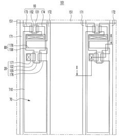
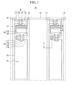
Organic light emitting diode (OLED) display
PatentActiveUS20110215302A1
Innovation
- The implementation of a translucent insulating layer filter on the encapsulation substrate, which forms a microcavity with the encapsulation substrate, reduces the need for fine metal masks by using separate patterned portions for each pixel and a continuous layer for all pixels, improving light efficiency and reducing mask usage.
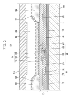
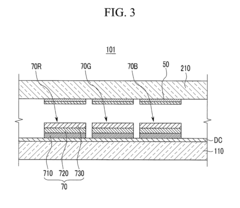
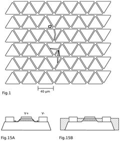
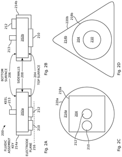
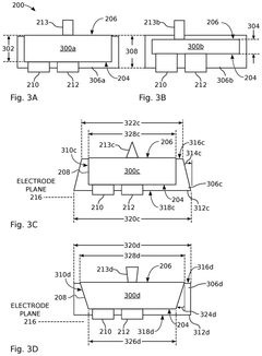
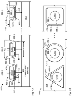
Encapsulated light emitting diodes for selective fluidic assembly
PatentActiveUS12119432B2
Innovation
- The use of partially encapsulated semiconductor-based inorganic micro-LEDs with a patternable polymer encapsulant that protects the LEDs from collisions and optimizes their shape for efficient assembly, allowing for higher speed and yield while preventing defects, and enabling precise alignment of LED colors on a display substrate.
Power Efficiency Comparison and Optimization
Power efficiency represents a critical differentiator between OLED and MicroLED display technologies, significantly influencing their respective image processing requirements and capabilities. OLED displays demonstrate variable power consumption patterns, with dark or black pixels consuming minimal to zero power, while bright pixels—particularly white ones—require substantially more energy. This characteristic necessitates specialized image processing algorithms that can optimize content to leverage OLED's power-saving potential through techniques like dark mode interfaces and strategic pixel dimming.
MicroLED technology, while still evolving, demonstrates promising efficiency metrics that potentially surpass OLED capabilities. Current research indicates MicroLED displays can achieve up to 30% greater energy efficiency at equivalent brightness levels compared to OLED panels. This efficiency stems from MicroLED's superior light emission mechanism, which converts more electrical energy directly into visible light with reduced heat generation.
The power efficiency profiles of these technologies directly impact image processing requirements. OLED systems benefit from Adaptive Brightness Control (ABC) algorithms that dynamically adjust pixel luminance based on content and ambient conditions, potentially reducing power consumption by 15-20% in typical usage scenarios. Conversely, MicroLED implementations require more sophisticated thermal management within their image processing pipelines due to their higher pixel density and concentrated heat generation characteristics.
Both technologies benefit from content-aware processing techniques. For OLED, this includes selective pixel dimming and color transformation algorithms that maintain perceived image quality while reducing power-intensive pixel states. MicroLED systems leverage similar approaches but with different optimization parameters due to their distinct electro-optical characteristics and more uniform power consumption across different color outputs.
Recent advancements in AI-driven image processing have introduced neural network models capable of real-time content analysis and power-optimized rendering. These systems can reduce display power consumption by an additional 10-15% through intelligent scene recognition and adaptive rendering techniques that preserve perceived visual quality while minimizing energy expenditure.
The industry is witnessing convergence in power management approaches across both technologies, with manufacturers implementing hybrid solutions that combine hardware-level efficiency improvements with software-based optimization. These integrated approaches typically include ambient light sensing, user behavior analysis, and content-adaptive processing to deliver optimal visual experiences with minimal power requirements.
Manufacturing Scalability and Cost Analysis
Manufacturing scalability represents a critical differentiator between OLED and MicroLED technologies, significantly impacting their respective market positions and future growth trajectories. OLED manufacturing has matured considerably over the past decade, with established production lines achieving economies of scale, particularly for small and medium-sized displays. Major manufacturers like Samsung and LG Display have invested billions in optimizing OLED production processes, reducing defect rates from over 50% to under 10% for certain panel sizes.
In contrast, MicroLED manufacturing faces substantial challenges in mass production. The process of transferring millions of microscopic LED chips precisely onto substrates remains a significant bottleneck. Current pick-and-place methods achieve transfer rates of approximately 150,000 units per hour, whereas commercial viability requires rates exceeding 10 million units per hour. This technical limitation directly impacts production yields and manufacturing costs.
Cost analysis reveals that OLED panels currently maintain a significant advantage, with production costs ranging from $100-150 per square foot for mainstream applications. MicroLED manufacturing costs remain prohibitively high at $600-1,000 per square foot, primarily due to low yields and complex assembly processes. Industry projections suggest MicroLED costs may decrease by 30-40% annually as manufacturing techniques improve, potentially reaching cost parity with premium OLED displays by 2027-2028.
The image processing implications of these manufacturing differences are substantial. OLED's established manufacturing ecosystem allows for more consistent pixel performance and color uniformity across production batches, simplifying downstream image processing requirements. MicroLED's manufacturing variability necessitates more sophisticated per-panel calibration and compensation algorithms to ensure visual consistency.
Energy efficiency in manufacturing also differs markedly between technologies. OLED production requires approximately 35-40% less energy per square meter compared to current MicroLED manufacturing processes, though this gap is expected to narrow as MicroLED techniques mature. This efficiency differential impacts not only production costs but also the environmental footprint of display technologies.
Regional manufacturing capabilities show distinct patterns, with East Asian countries dominating OLED production capacity (over 90% of global output), while MicroLED manufacturing expertise is more distributed globally, with significant research clusters in North America and Europe alongside Asian production facilities. This geographical distribution influences supply chain resilience and technology development pathways for image processing solutions built around these display technologies.
Unlock deeper insights with PatSnap Eureka Quick Research — get a full tech report to explore trends and direct your research. Try now!
Generate Your Research Report Instantly with AI Agent
Supercharge your innovation with PatSnap Eureka AI Agent Platform!