OLED vs MicroLED: Semiconductor Material Advances
OCT 24, 20259 MIN READ
Generate Your Research Report Instantly with AI Agent
Patsnap Eureka helps you evaluate technical feasibility & market potential.
Display Technology Evolution and Objectives
Display technology has undergone remarkable evolution since the introduction of cathode ray tubes (CRTs) in the early 20th century. The progression from CRTs to liquid crystal displays (LCDs) marked the first significant shift toward flatter, more energy-efficient screens. The subsequent development of plasma display panels offered improved contrast and viewing angles but remained energy-intensive. The introduction of OLED (Organic Light-Emitting Diode) technology in the early 2000s represented a revolutionary advancement, enabling thinner, lighter displays with superior color reproduction and perfect blacks.
The current technological battleground centers on OLED versus MicroLED technologies, with both representing the cutting edge of display innovation. OLED technology utilizes organic compounds that emit light when electricity is applied, eliminating the need for backlighting. This results in displays with exceptional contrast ratios, wide viewing angles, and the ability to create flexible and transparent screens. However, OLED faces challenges including limited lifespan, particularly for blue subpixels, and susceptibility to burn-in effects.
MicroLED technology, emerging as OLED's primary competitor, employs inorganic gallium nitride (GaN) semiconductor materials to create microscopic LED arrays. These displays promise even better brightness, energy efficiency, and longevity than OLEDs while maintaining comparable contrast ratios and color reproduction. The fundamental difference lies in the semiconductor materials: organic compounds for OLED versus inorganic materials for MicroLED, with significant implications for manufacturing processes, performance characteristics, and application suitability.
Recent advancements in semiconductor materials have accelerated the development trajectory for both technologies. For OLED, innovations in phosphorescent and thermally activated delayed fluorescence (TADF) materials have improved efficiency and lifespan. Meanwhile, MicroLED research has focused on overcoming mass transfer challenges and reducing the size of individual LED elements while maintaining brightness uniformity.
The primary objectives driving display technology evolution include achieving higher energy efficiency, extended operational lifespan, improved brightness and contrast ratios, enhanced color gamut coverage, and reduced manufacturing costs. Additional goals include developing environmentally sustainable production methods and materials, as well as enabling novel form factors such as foldable, rollable, and transparent displays.
Looking forward, the industry aims to overcome current technical limitations through continued semiconductor material innovation. For OLED, this means developing more stable blue emitters and improving encapsulation techniques to prevent degradation. For MicroLED, objectives include perfecting mass transfer techniques for smaller pixel sizes and reducing production costs to enable mainstream adoption across various device categories.
Market Demand Analysis for Advanced Display Technologies
The display technology market is experiencing a significant shift as advanced technologies like OLED and MicroLED compete for dominance. Current market analysis indicates that the global display market is projected to reach $167 billion by 2025, with OLED and MicroLED technologies representing the fastest-growing segments. Consumer electronics, particularly smartphones and televisions, remain the primary drivers of demand, accounting for approximately 65% of the total market share.
OLED technology has established a strong market presence with widespread adoption in premium smartphones and high-end televisions. Samsung and LG Display have capitalized on this trend, securing substantial market shares in the OLED segment. The automotive industry represents an emerging market for OLED displays, with luxury vehicle manufacturers increasingly incorporating these displays in dashboard systems and entertainment consoles.
MicroLED, though still in earlier commercialization stages, is generating substantial interest from both manufacturers and consumers. Market research indicates growing demand for MicroLED in specialized applications requiring exceptional brightness, durability, and energy efficiency. The technology is particularly appealing for large-format displays, AR/VR devices, and premium consumer electronics where performance justifies the higher cost.
Regional analysis reveals that Asia-Pacific dominates the advanced display manufacturing landscape, with South Korea, Japan, and Taiwan leading in production capacity. However, North America and Europe represent significant consumer markets, particularly for premium display technologies. China is rapidly expanding its manufacturing capabilities in both OLED and MicroLED, potentially reshaping market dynamics in the coming years.
Consumer preference surveys indicate increasing awareness and demand for display quality, with brightness, color accuracy, and energy efficiency emerging as key purchasing factors. The premium segment of consumers has demonstrated willingness to pay 20-30% more for superior display technologies, creating viable market opportunities for both OLED and MicroLED solutions.
Industry forecasts suggest that semiconductor material advances will be critical in determining market penetration rates for these technologies. Innovations in quantum dot materials for OLED and gallium nitride substrates for MicroLED are expected to significantly impact production costs and performance metrics, potentially accelerating adoption rates across various application sectors.
The commercial viability of MicroLED technology hinges on manufacturing scale economies, with current production costs remaining prohibitively high for mass-market applications. However, market analysts predict that continued semiconductor material innovations could reduce production costs by 40-50% within the next five years, potentially triggering widespread adoption across multiple product categories.
OLED and MicroLED Technical Challenges
Both OLED and MicroLED technologies face significant technical challenges that impact their commercial viability and performance capabilities. OLED displays continue to struggle with limited operational lifespans, particularly for blue emitters which typically degrade faster than red and green counterparts. This differential aging leads to color shift over time, compromising display quality. The organic materials in OLEDs remain susceptible to moisture and oxygen, necessitating complex encapsulation techniques that add to manufacturing complexity and cost.
Material stability represents another critical challenge for OLED technology. The organic compounds used in these displays are inherently less stable than inorganic alternatives, resulting in burn-in issues when static images are displayed for extended periods. Additionally, OLED manufacturing processes require precise deposition of multiple organic layers, with even minor contamination potentially causing significant defects.
MicroLED technology, while promising, faces its own set of formidable challenges. The most significant hurdle is the mass transfer process required to place millions of tiny LED chips precisely onto display substrates. Current yield rates remain problematic, with even small percentages of defective transfers resulting in visible display imperfections. The industry has yet to develop a universally effective mass transfer technique that balances speed, accuracy, and cost-effectiveness at production scale.
Miniaturization presents another substantial challenge for MicroLED development. As manufacturers push toward higher resolution displays, individual LED sizes must decrease to sub-10 micron dimensions. At these scales, quantum efficiency tends to decline due to increased surface defects relative to chip volume, requiring novel semiconductor engineering approaches to maintain brightness and efficiency.
Color conversion efficiency remains problematic for both technologies. MicroLED displays typically use blue LEDs with phosphor or quantum dot conversion layers for red and green pixels, introducing energy losses during conversion. Meanwhile, OLED displays struggle with different efficiency levels across color emitters, with blue consistently underperforming compared to red and green.
Power efficiency under real-world usage conditions continues to challenge both technologies. While OLEDs offer theoretical power advantages for dark content due to their emissive nature, they suffer efficiency losses at high brightness levels. MicroLEDs demonstrate excellent peak brightness efficiency but may consume more power for typical content with mixed brightness levels.
Manufacturing scalability represents perhaps the most significant barrier to widespread MicroLED adoption. Current production methods remain prohibitively expensive for consumer applications, with costs significantly higher than mature OLED manufacturing. The industry must develop new approaches to epitaxial growth, chip separation, and inspection to achieve economically viable production scales.
Current Semiconductor Materials for OLED and MicroLED
01 OLED semiconductor materials and structures
Organic Light Emitting Diode (OLED) technology utilizes organic semiconductor materials that emit light when an electric current is applied. These materials are typically arranged in a multilayer structure including emission layers, transport layers, and electrodes. Advanced OLED designs incorporate various organic compounds and dopants to achieve specific color outputs, brightness levels, and energy efficiency. Recent innovations focus on improving the stability and lifetime of these organic materials while reducing power consumption.- OLED semiconductor materials and structures: Organic Light Emitting Diode (OLED) technology utilizes organic semiconductor materials that emit light when an electric current is applied. These materials are typically arranged in a multilayer structure including emission layers, electron transport layers, and hole transport layers. Advanced OLED semiconductor materials include phosphorescent compounds and thermally activated delayed fluorescence (TADF) materials that improve efficiency and color purity. The structure often incorporates specialized electrodes and encapsulation to protect the organic materials from environmental degradation.
- MicroLED semiconductor materials and fabrication: MicroLED display technology uses inorganic semiconductor materials, primarily gallium nitride (GaN) based compounds, to create microscopic LED arrays. These materials offer advantages including higher brightness, longer lifespan, and better energy efficiency compared to organic alternatives. The fabrication process involves epitaxial growth of semiconductor layers on substrates, followed by precise patterning and transfer techniques to position the micro-scale LEDs. Innovations in this field focus on improving the yield of the transfer process and developing more efficient semiconductor structures.
- Quantum dot enhancement for display technologies: Quantum dots are semiconductor nanocrystals that can be incorporated into both OLED and MicroLED displays to enhance color performance. These nanomaterials, typically made from materials such as cadmium selenide or indium phosphide, can be precisely tuned to emit specific wavelengths of light by controlling their size. When integrated into display technologies, quantum dots improve color gamut, brightness, and energy efficiency. Recent developments include cadmium-free quantum dots and integration methods that preserve the stability and performance of these nanomaterials in display applications.
- Flexible and transparent display semiconductor materials: Advanced semiconductor materials enable the development of flexible and transparent OLED and MicroLED displays. These include specialized substrate materials such as polyimide films, transparent conductive oxides like indium tin oxide (ITO), and novel electrode materials. The semiconductor layers are engineered to maintain performance under mechanical stress, allowing for bendable, foldable, or rollable displays. Transparent display technologies utilize materials with high optical transparency while maintaining electrical conductivity, enabling applications in augmented reality and smart windows.
- Integration technologies for display systems: Integration technologies for OLED and MicroLED displays focus on combining semiconductor materials with driving circuits and other system components. These include thin-film transistor (TFT) backplanes made from materials such as low-temperature polysilicon (LTPS) or oxide semiconductors, which control individual pixels. Advanced integration approaches incorporate sensors, signal processing circuits, and power management systems directly into the display structure. Recent innovations include monolithic integration techniques that reduce manufacturing complexity and improve display performance through closer coupling of semiconductor components.
02 MicroLED semiconductor materials and fabrication
MicroLED technology employs inorganic semiconductor materials, primarily gallium nitride (GaN) based compounds, to create extremely small LED structures. These microscopic LEDs offer advantages in brightness, energy efficiency, and longevity compared to traditional display technologies. The fabrication process involves epitaxial growth of semiconductor layers, followed by precise patterning and transfer techniques to position the microLEDs on display substrates. Recent developments focus on improving mass transfer methods and reducing defect rates during manufacturing.Expand Specific Solutions03 Quantum dot enhancement for display technologies
Quantum dots are semiconductor nanocrystals that can be incorporated into both OLED and MicroLED displays to enhance color performance. These nanomaterials can be precisely tuned to emit specific wavelengths of light by controlling their size and composition. When integrated with display technologies, quantum dots improve color gamut, brightness, and energy efficiency. Recent innovations focus on developing cadmium-free quantum dots and improving their stability and integration methods with existing display architectures.Expand Specific Solutions04 Flexible and transparent display materials
Advanced semiconductor materials enable the development of flexible and transparent displays for both OLED and MicroLED technologies. These materials include specialized substrates, transparent conductive oxides, and novel encapsulation layers that maintain performance while allowing bending or transparency. Flexible displays utilize thin-film transistor backplanes on polymer substrates, while transparent displays incorporate materials with high optical transmittance. Recent developments focus on improving durability during repeated flexing and enhancing optical clarity while maintaining electrical performance.Expand Specific Solutions05 Hybrid and novel semiconductor architectures
Innovative semiconductor architectures combine elements of different display technologies to leverage their respective advantages. These hybrid approaches include integrating quantum dot color conversion layers with MicroLED backplanes, developing tandem OLED structures with multiple emission layers, and creating composite semiconductor materials with enhanced electrical and optical properties. Novel architectures also explore alternative charge transport mechanisms and emission processes to improve efficiency and reduce power consumption while maintaining high display quality.Expand Specific Solutions
Key Industry Players and Competitive Landscape
The OLED vs MicroLED semiconductor material landscape is evolving through a competitive transition phase, with the market projected to reach $200+ billion by 2025. OLED technology, championed by established players like Samsung Electronics, LG Electronics, and Universal Display Corporation, has achieved commercial maturity with widespread adoption in consumer electronics. Meanwhile, MicroLED represents the emerging frontier, with companies like Apple, BOE Technology, and Intel investing heavily in R&D to overcome manufacturing challenges. The technology competition centers on advancements in semiconductor materials, with Universal Display and Merck leading OLED material innovation, while Samsung, BOE, and Applied Materials focus on developing more efficient MicroLED fabrication processes and novel semiconductor compounds to enable higher brightness, lower power consumption, and improved durability.
BOE Technology Group Co., Ltd.
Technical Solution: BOE has developed comprehensive solutions for both OLED and MicroLED technologies. In OLED, BOE has created flexible AMOLED displays using low-temperature polysilicon (LTPS) backplanes that enable higher electron mobility and better power efficiency. Their semiconductor material innovations include soluble OLED materials that can be applied using inkjet printing methods, potentially reducing manufacturing costs by up to 30% compared to traditional vacuum deposition techniques. For MicroLED, BOE has developed a mass transfer process capable of handling ultra-small LED chips (under 30 micrometers) with high precision placement. Their semiconductor material research focuses on improving the efficiency of GaN-based LED chips, particularly for red wavelengths which traditionally suffer from lower efficiency. BOE has also created novel thin-film transistor architectures using oxide semiconductors that provide better current uniformity across MicroLED arrays, addressing one of the key challenges in achieving consistent brightness in these displays.
Strengths: BOE possesses strong manufacturing scale with multiple production lines capable of supporting both technologies, and they have developed cost-effective approaches for OLED production. Weaknesses: Their MicroLED technology still faces significant commercialization hurdles, particularly in achieving the yields necessary for consumer products, and they have less experience with phosphorescent OLED materials compared to some competitors.
Samsung Electronics Co., Ltd.
Technical Solution: Samsung has pioneered significant advancements in both OLED and MicroLED technologies. For OLED, Samsung has developed quantum dot (QD)-OLED technology that combines quantum dots with blue OLED emitters to achieve superior color purity and brightness. Their semiconductor material innovations include vapor deposition techniques for more uniform OLED layers and the use of phosphorescent materials to improve energy efficiency by up to 25%. In MicroLED development, Samsung has created transfer technologies capable of precisely placing microscopic LED chips (under 50 micrometers) onto display substrates with high accuracy. They've developed gallium nitride (GaN)-based semiconductor materials with improved luminous efficiency and have implemented innovative thin-film transistor (TFT) backplanes that enable higher pixel densities. Samsung's "The Wall" MicroLED display showcases these advancements with modular design capabilities and exceptional brightness exceeding 2,000 nits.
Strengths: Samsung possesses comprehensive vertical integration from semiconductor materials to finished displays, allowing for optimized material development. Their extensive patent portfolio in both technologies provides competitive advantage. Weaknesses: Their MicroLED mass production techniques still face yield challenges, and the high manufacturing costs limit market penetration compared to their established OLED business.
Core Material Innovations and Patent Analysis
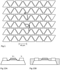
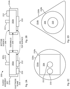
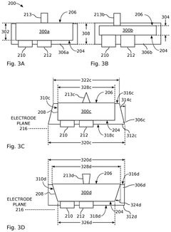
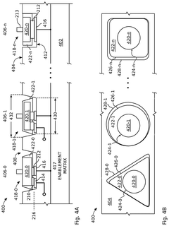
Encapsulated light emitting diodes for selective fluidic assembly
PatentActiveUS12119432B2
Innovation
- The use of partially encapsulated semiconductor-based inorganic micro-LEDs with a patternable polymer encapsulant that protects the LEDs from collisions and optimizes their shape for efficient assembly, allowing for higher speed and yield while preventing defects, and enabling precise alignment of LED colors on a display substrate.
Anisotropic conductive film and display device
PatentActiveUS20220102326A1
Innovation
- An anisotropic conductive film with a first region of discretely arranged conductive particles corresponding to electrode patterns and a second region with aggregated conductive particles acting as an alignment marker, facilitating easy alignment with the circuit substrate and reducing production costs by forming alignment markers through conductive particle dispersion.
Manufacturing Process Comparison
The manufacturing processes for OLED and MicroLED displays represent significantly different approaches to creating advanced display technologies, each with distinct advantages and challenges. OLED manufacturing has matured considerably over the past decade, utilizing vacuum thermal evaporation for small molecule OLEDs and solution processing techniques for polymer-based variants. The process typically involves depositing multiple organic layers onto a substrate, with precise thickness control in the nanometer range. This approach benefits from established infrastructure but faces yield challenges at larger screen sizes due to pixel defects.
MicroLED manufacturing, by contrast, remains in earlier stages of industrial development, employing semiconductor fabrication techniques similar to those used in LED production. The critical distinction lies in the mass transfer process required to place millions of microscopic LED chips precisely onto display substrates. This mass transfer represents the most significant manufacturing hurdle for MicroLED technology, with various approaches under development including stamp transfer, laser transfer, and fluid-assisted methods.
Equipment requirements differ substantially between these technologies. OLED production relies heavily on specialized vacuum deposition chambers and encapsulation systems to protect the organic materials from environmental degradation. MicroLED manufacturing demands high-precision placement equipment capable of positioning components with micron-level accuracy and throughput sufficient for commercial viability.
Cost structures also diverge significantly. OLED manufacturing has benefited from economies of scale, particularly for smartphone-sized displays, though larger formats remain costly. The primary expense drivers include material costs and yield management. MicroLED production currently faces higher costs due to the complexity of the mass transfer process and the early stage of equipment development, though theoretical cost advantages exist if manufacturing challenges can be overcome.
Environmental considerations present another point of differentiation. OLED manufacturing involves organic solvents and potential waste issues, while MicroLED production utilizes more traditional semiconductor materials but may require greater energy inputs. Both technologies are pursuing more sustainable manufacturing approaches, including reduced material waste and energy consumption.
The manufacturing scalability trajectories differ markedly. OLED technology has demonstrated successful scaling for small to medium displays but faces increasing challenges with larger formats. MicroLED shows promise for eventual superior scalability across all size ranges once mass transfer technologies mature, potentially offering more flexible production capabilities in the future.
Energy Efficiency and Environmental Impact
Energy efficiency has emerged as a critical differentiator between OLED and MicroLED display technologies, with significant implications for both consumer applications and environmental sustainability. OLED displays currently dominate the premium smartphone and high-end television markets partly due to their energy efficiency advantages in displaying dark content. This efficiency stems from OLED's fundamental operating principle—pixels emit light only when needed and consume minimal power when displaying black.
MicroLED technology, while still evolving, demonstrates promising energy efficiency characteristics that may eventually surpass OLED. Recent semiconductor material advances have focused on improving the external quantum efficiency (EQE) of MicroLED emitters. Notably, research from Seoul National University has achieved EQE improvements of up to 27% through novel quantum dot integration techniques, potentially reducing power consumption by 30-40% compared to current commercial OLED panels.
The environmental impact assessment of these technologies reveals important distinctions throughout their lifecycles. OLED manufacturing processes typically involve organic solvents and potentially hazardous materials like iridium complexes, raising concerns about waste management and resource scarcity. The production process also requires significant energy inputs, with estimates suggesting that manufacturing a single OLED panel consumes approximately 150-200 kWh of electricity.
MicroLED fabrication presents different environmental challenges, particularly in the epitaxial growth processes for III-V semiconductor materials. However, recent advances in gallium nitride (GaN) on silicon substrates have reduced both material costs and environmental footprint. Samsung's research division has reported a 35% reduction in process chemicals through optimized manufacturing techniques for their next-generation MicroLED displays.
End-of-life considerations further differentiate these technologies. OLED panels contain organic materials that degrade over time, with an average lifespan of 30,000-50,000 hours before significant brightness reduction occurs. MicroLED displays potentially offer longer operational lifespans exceeding 100,000 hours, which could significantly reduce electronic waste generation over time. Additionally, the inorganic nature of MicroLED materials may facilitate more straightforward recycling processes.
Carbon footprint analyses conducted by independent research firms indicate that the lifetime energy consumption difference between these technologies could be substantial. A 55-inch MicroLED television is projected to consume approximately 30% less energy over a 10-year lifespan compared to equivalent OLED models, translating to approximately 300-400 kg less CO2 emissions per unit, assuming average global electricity generation carbon intensities.
Unlock deeper insights with Patsnap Eureka Quick Research — get a full tech report to explore trends and direct your research. Try now!
Generate Your Research Report Instantly with AI Agent
Supercharge your innovation with Patsnap Eureka AI Agent Platform!