

OLED vs MicroLED: Strategic Insights into Material Usage
OCT 24, 202510 MIN READ
Generate Your Research Report Instantly with AI Agent
PatSnap Eureka helps you evaluate technical feasibility & market potential.
Display Technology Evolution and Objectives
Display technology has undergone remarkable evolution since the introduction of cathode ray tubes (CRTs) in the early 20th century. The progression from CRTs to liquid crystal displays (LCDs) marked the first major shift toward flatter, more energy-efficient screens. This transition was followed by the development of plasma display panels, which offered improved contrast ratios and viewing angles but struggled with power consumption issues.
The introduction of Organic Light-Emitting Diode (OLED) technology in the late 1990s represented a paradigm shift in display technology. Unlike LCDs that require backlighting, OLED pixels emit their own light when an electric current is applied, enabling thinner displays with superior contrast ratios, wider viewing angles, and faster response times. OLED technology has since dominated high-end smartphones and premium television markets.
MicroLED technology emerged as a promising next-generation display solution in the mid-2010s. Building upon the self-emissive principle of OLEDs, MicroLEDs utilize inorganic gallium nitride (GaN) materials instead of organic compounds. This fundamental material difference addresses several limitations of OLED technology, including shorter lifespan, burn-in issues, and brightness constraints.
The current technological competition between OLED and MicroLED centers significantly on material usage and efficiency. OLED displays utilize organic compounds that can be deposited through relatively mature processes like vacuum thermal evaporation or solution processing. In contrast, MicroLED fabrication involves more complex semiconductor manufacturing techniques, presenting both challenges and opportunities for material innovation.
The primary objective in this technological evolution is to develop display technologies that optimize the balance between visual performance, energy efficiency, manufacturing scalability, and cost-effectiveness. OLED technology has achieved significant market penetration due to its mature manufacturing processes and excellent visual characteristics, while MicroLED promises superior brightness, longevity, and efficiency but faces manufacturing complexity hurdles.
Material usage represents a critical strategic consideration in this technological competition. OLED displays require rare and expensive materials such as iridium for phosphorescent emitters, while MicroLED technology relies on semiconductor materials like gallium nitride that present different supply chain considerations. The environmental impact of these materials, including extraction, processing, and end-of-life disposal, is becoming increasingly important in strategic technology planning.
The industry aims to develop display technologies that reduce reliance on scarce materials while maintaining or improving performance characteristics. This includes research into alternative emitter materials for OLEDs and more efficient manufacturing processes for MicroLEDs that minimize material waste. The ultimate goal is to create display technologies that deliver exceptional visual experiences while addressing sustainability concerns and manufacturing scalability.
Market Demand Analysis for Advanced Display Technologies
The display technology market is witnessing unprecedented growth driven by increasing consumer demand for superior visual experiences across multiple device categories. Current market analysis indicates that the global advanced display market is projected to reach $167 billion by 2025, with OLED technology currently dominating premium segments while MicroLED emerges as a promising contender. This growth trajectory is supported by expanding applications in smartphones, televisions, wearables, automotive displays, and commercial signage.
Consumer preferences are increasingly favoring thinner, more energy-efficient displays with higher resolution, better color accuracy, and longer lifespans. OLED technology has successfully captured the high-end smartphone market, with approximately 500 million OLED smartphone displays shipped annually. Meanwhile, the television segment shows growing consumer willingness to pay premium prices for advanced display technologies, particularly in the 55-inch and larger categories where visual quality differences become more apparent.
The automotive industry represents a rapidly expanding market for advanced displays, with projections indicating a 20% annual growth rate for in-vehicle display implementations. Both OLED and MicroLED technologies are positioned to address this sector's unique requirements for durability, brightness, and operational temperature range. The automotive display market values these technologies' ability to maintain visibility in varying lighting conditions while conforming to curved and irregular surfaces within vehicle interiors.
Commercial and public display applications constitute another significant market segment, with digital signage and large-format displays requiring technologies that offer superior brightness, energy efficiency, and outdoor visibility. MicroLED's advantages in these areas position it favorably for capturing market share in this segment, which is growing at 15% annually.
Regional market analysis reveals varying adoption patterns, with East Asian markets leading in both production capacity and consumer adoption of advanced display technologies. North American and European markets demonstrate strong premium segment demand, while emerging economies show accelerating adoption rates as manufacturing costs decrease and technology becomes more accessible.
Material supply chain considerations are increasingly influencing market dynamics, with rare earth elements used in MicroLED production facing potential supply constraints. Similarly, specialized organic compounds required for OLED manufacturing represent a critical factor in production scaling and cost reduction efforts. These material considerations are becoming central to strategic planning for display manufacturers and their component suppliers.
The market is also responding to sustainability concerns, with consumers and regulatory bodies increasingly favoring technologies with lower environmental impacts throughout their lifecycle. This trend benefits technologies that reduce material usage, extend product lifespan, and facilitate end-of-life recycling – factors that will increasingly influence consumer purchasing decisions and corporate investment strategies in display technology development.
OLED and MicroLED Technical Challenges
Both OLED and MicroLED display technologies face significant technical challenges that impact their commercial viability and market adoption. OLED technology, despite being more mature in the market, continues to struggle with several persistent issues. The organic materials in OLED displays are susceptible to degradation over time, particularly blue emitters which have shorter lifespans compared to red and green counterparts. This differential aging leads to color shift and reduced display quality over the product lifecycle.
Manufacturing yield remains problematic for OLED, especially for larger panels where defect rates increase exponentially with size. The complex multi-layer deposition process requires extremely precise control of layer thickness and uniformity, with even minor variations causing visible defects. Additionally, OLED displays suffer from burn-in issues when static images are displayed for extended periods, limiting their application in scenarios requiring constant information display.
MicroLED technology, while promising superior performance, faces even more formidable manufacturing challenges. The most significant hurdle is the mass transfer process - moving millions of tiny LED chips from the growth substrate to the display backplane with perfect precision. Current pick-and-place technologies struggle with the throughput requirements for commercial production, creating a major bottleneck in manufacturing scalability.
Yield management presents another critical challenge for MicroLED. With displays containing millions of individual LEDs, achieving acceptable defect rates requires unprecedented manufacturing precision. Even a small percentage of defective pixels becomes visually significant across a full display. The repair processes for defective pixels are complex and time-consuming, further impacting production costs.
Size uniformity of MicroLED chips presents additional complications. As manufacturers push toward smaller LED sizes to increase resolution, maintaining consistent performance across millions of elements becomes increasingly difficult. Variations in chip size affect brightness, color accuracy, and power efficiency across the display.
Both technologies face efficiency challenges, though in different ways. OLED struggles with power consumption, particularly when displaying bright content, while MicroLED faces challenges in light extraction efficiency and electrical-to-optical conversion rates. Heat management also remains problematic for both technologies, with thermal issues affecting both performance and longevity.
Material sourcing represents another shared challenge. OLED requires specialized organic compounds with strict purity requirements, while MicroLED depends on high-quality semiconductor materials and precise doping processes. Supply chain stability for these specialized materials impacts production costs and manufacturing reliability for both technologies.
Current Material Solutions for OLED and MicroLED
01 Organic materials for OLED displays
Organic light-emitting diode (OLED) displays utilize various organic materials as the emissive electroluminescent layer. These materials include polymers and small molecules that emit light when an electric current is applied. The organic compounds are typically arranged in layers, including hole transport layers, emission layers, and electron transport layers. The selection and arrangement of these organic materials significantly impact the display's efficiency, color accuracy, and lifespan.- Organic materials for OLED displays: Organic light-emitting diode (OLED) displays utilize various organic materials as the emissive electroluminescent layer. These materials include organic compounds that emit light when an electric current is applied. The organic layers typically consist of a hole transport layer, an emissive layer, and an electron transport layer. Different organic materials are selected based on their emission wavelengths to produce different colors. These materials offer advantages such as flexibility, thinness, and energy efficiency in display applications.
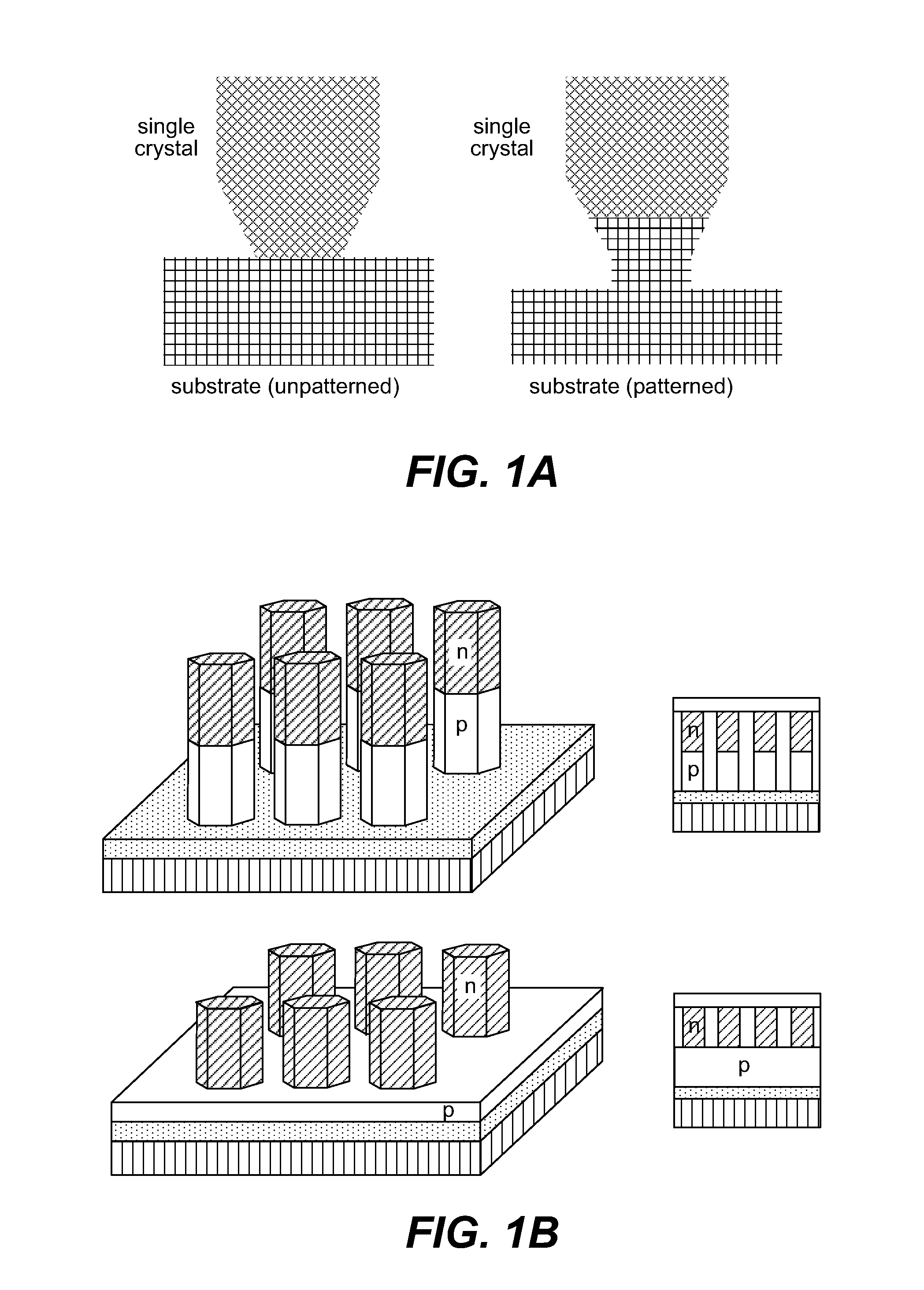
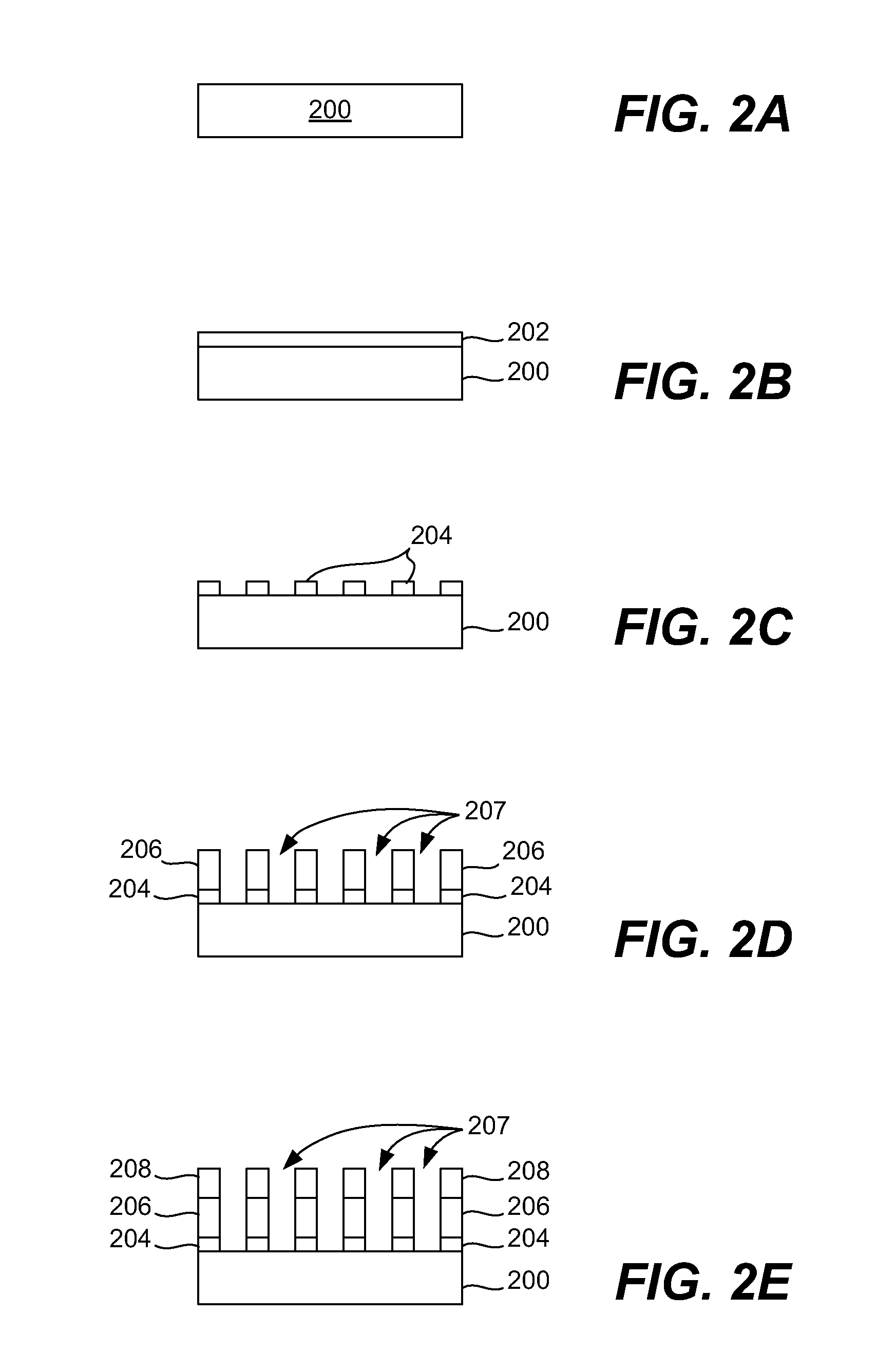
- Inorganic materials for MicroLED displays: MicroLED displays utilize inorganic semiconductor materials, primarily gallium nitride (GaN) based compounds, to create extremely small light-emitting diodes. These materials provide high brightness, excellent color saturation, and long lifespans. The inorganic nature of MicroLEDs offers advantages over OLEDs including higher durability, better resistance to burn-in, and superior performance in high-brightness environments. The manufacturing process involves epitaxial growth of these semiconductor materials and subsequent transfer to display substrates.
- Substrate and encapsulation materials: Both OLED and MicroLED technologies require specialized substrate and encapsulation materials to protect the sensitive display components from environmental factors such as moisture and oxygen. These materials include glass, flexible polymers, metal foils, and thin-film encapsulation layers. Advanced barrier films with multiple inorganic and organic layers are used to achieve the required protection while maintaining flexibility in certain applications. The choice of substrate and encapsulation materials significantly impacts the display's durability, flexibility, and optical performance.
- Electrode and conductive materials: Electrode and conductive materials play a crucial role in both OLED and MicroLED display technologies. These include transparent conductive oxides like indium tin oxide (ITO), metal nanowires, graphene, and various metal alloys. The electrodes must balance conductivity with transparency to allow light to pass through while efficiently delivering current to the emissive materials. Advanced electrode designs incorporate novel materials and structures to improve current distribution, reduce resistance, and enhance overall display performance while enabling features like flexibility and transparency.
- Color conversion and quantum dot materials: Color conversion materials are increasingly important in both OLED and MicroLED display technologies. Quantum dots, phosphors, and other color conversion materials can be used to convert blue or UV light into precise wavelengths for red and green colors, enabling more efficient and accurate color reproduction. These materials allow for wider color gamuts and improved energy efficiency. The integration of quantum dots with MicroLEDs is particularly promising, as it combines the efficiency and brightness of MicroLEDs with the color purity of quantum dots, potentially reducing manufacturing complexity.
02 Inorganic materials for MicroLED displays
MicroLED displays employ inorganic semiconductor materials, primarily gallium nitride (GaN) based compounds, to create extremely small light-emitting diodes. These materials offer advantages such as higher brightness, better energy efficiency, and longer lifespans compared to organic counterparts. The manufacturing process involves growing epitaxial layers on substrates like sapphire or silicon, followed by precise patterning and transfer techniques to position the microscopic LEDs on display backplanes.Expand Specific Solutions03 Substrate and backplane materials
Both OLED and MicroLED technologies rely on various substrate and backplane materials that serve as the foundation for the display structure. Common substrate materials include glass, flexible polymers for bendable displays, and rigid silicon. The backplane, which contains the driving circuitry, typically uses thin-film transistors (TFTs) made from materials such as low-temperature polysilicon (LTPS), indium gallium zinc oxide (IGZO), or amorphous silicon. The choice of substrate and backplane materials affects display flexibility, resolution, and manufacturing complexity.Expand Specific Solutions04 Encapsulation and protective materials
Encapsulation materials play a crucial role in protecting both OLED and MicroLED displays from environmental factors such as moisture and oxygen, which can degrade performance. Advanced thin-film encapsulation techniques use alternating layers of inorganic (silicon nitride, aluminum oxide) and organic materials to create effective barriers. For MicroLEDs, additional protective coatings may be applied to enhance durability and optical performance. These materials significantly impact the longevity and reliability of the display technologies.Expand Specific Solutions05 Color conversion and enhancement materials
Both display technologies utilize various materials for color conversion and enhancement. In OLED displays, color filters and phosphorescent materials are employed to achieve a wide color gamut. MicroLED displays often incorporate quantum dots or phosphor materials to convert blue or UV light into different colors, reducing the need for separate red, green, and blue LED fabrication. Additionally, specialized optical films and coatings are used to improve light extraction efficiency, reduce reflections, and enhance contrast ratios in both technologies.Expand Specific Solutions
Key Industry Players and Competitive Landscape
The OLED vs MicroLED display technology landscape is currently in a transitional phase, with OLED being mature and commercially established while MicroLED remains in early commercialization. The global market for these advanced display technologies is projected to reach $200+ billion by 2025, driven by demand for higher performance displays in consumer electronics and automotive applications. In terms of technical maturity, companies like Samsung Display, LG Display, and BOE have established OLED manufacturing capabilities, while MicroLED development is being pursued by Samsung, Apple, and specialized players like X Display Co. Material innovation remains critical, with Universal Display Corporation leading in OLED materials research while companies like Lumileds and Applied Materials are developing specialized solutions for MicroLED manufacturing challenges, particularly in mass transfer techniques and miniaturization.
BOE Technology Group Co., Ltd.
Technical Solution: BOE has developed a comprehensive portfolio of display technologies spanning both OLED and MicroLED domains with distinct material strategies. For OLED, BOE has pioneered a flexible printed OLED manufacturing process that reduces material consumption by approximately 20% compared to traditional vapor deposition methods[1]. Their proprietary "crystal silicon OLED" technology incorporates oxide TFT backplanes that improve electron mobility while requiring fewer rare earth elements than conventional approaches. In the MicroLED space, BOE has focused on developing glass-based transfer substrates that enable simultaneous transfer of multiple microLED chips, significantly improving production efficiency and reducing material waste[2]. Their "active matrix MicroLED" architecture employs a unique pixel circuit design that minimizes the required semiconductor material while maintaining brightness uniformity. BOE has also made significant advances in quantum dot color conversion layers for both technologies, developing cadmium-free materials that achieve over 90% of the DCI-P3 color gamut while meeting environmental regulations[3]. Additionally, BOE has invested in thin-film encapsulation techniques that reduce barrier material requirements by approximately 30% while maintaining moisture protection comparable to traditional glass encapsulation[4].
Strengths: BOE's printed OLED approach offers cost advantages and material efficiency improvements for mass production. Their batch transfer process for MicroLED shows promise for scaling to larger displays with higher yields than single-chip transfers. Weaknesses: BOE's OLED material quality and lifetime metrics still lag behind Samsung and LG, particularly for mobile applications. Their MicroLED technology faces challenges in achieving consistent color uniformity across large panels due to material variations in the transfer process.
Universal Display Corp.
Technical Solution: Universal Display Corporation (UDC) has established itself as the preeminent developer of phosphorescent OLED (PHOLED) materials, which form the foundation of most commercial OLED displays today. Their proprietary emitter materials achieve nearly 100% internal quantum efficiency compared to 25% for fluorescent materials, dramatically reducing power consumption and extending device lifetimes[1]. UDC's latest generation of emitter materials incorporates novel metal-organic complexes that have improved blue PHOLED stability by over 50% compared to previous generations, addressing one of the industry's most persistent challenges[2]. While not directly manufacturing MicroLED materials, UDC has developed complementary technologies that bridge both display approaches, including OVJP (Organic Vapor Jet Printing) that enables direct patterning of OLED materials without shadow masks, reducing material waste by up to 90% compared to traditional vapor deposition methods[3]. Their UniversalBarrier encapsulation technology provides ultra-low moisture permeation for flexible displays while using significantly thinner material layers than conventional approaches. UDC has also pioneered soluble OLED materials that enable solution processing methods, potentially allowing for more efficient manufacturing with less material waste than vacuum deposition techniques[4].
Strengths: UDC maintains unparalleled expertise in phosphorescent emitter chemistry with an extensive patent portfolio that makes them essential partners for all major OLED manufacturers. Their OVJP technology offers a potential breakthrough in material efficiency for OLED production. Weaknesses: UDC remains heavily dependent on the OLED market with limited diversification into MicroLED materials. Their blue PHOLED materials still face lifetime challenges despite improvements, requiring display manufacturers to make compromises in color balance or brightness.
Critical Patents and Innovations in Display Materials
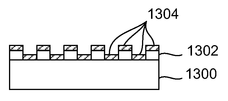
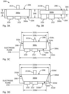
Micro- and NANO-structured LED and OLED devices
PatentInactiveUS20110168976A1
Innovation
- The use of micro- or nano-structured features in LED and OLED devices, achieved through nanoscale heteroepitaxy and ultrafast laser-based doping, reduces lattice strain, improves p-doping, and facilitates carrier injection and recombination, confining current flow and providing internal light guiding for enhanced efficiency.

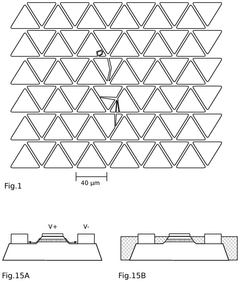
Encapsulated light emitting diodes for selective fluidic assembly
PatentActiveUS12119432B2
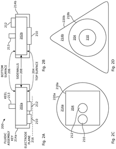
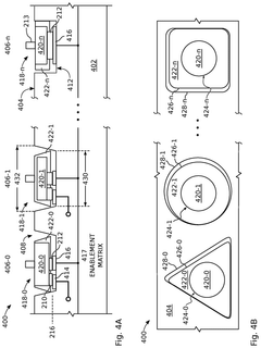
Innovation
- The use of partially encapsulated semiconductor-based inorganic micro-LEDs with a patternable polymer encapsulant that protects the LEDs from collisions and optimizes their shape for efficient assembly, allowing for higher speed and yield while preventing defects, and enabling precise alignment of LED colors on a display substrate.
Supply Chain Analysis and Material Sourcing Strategies
The supply chain for display technologies represents a critical factor in determining both the commercial viability and environmental impact of OLED and MicroLED technologies. OLED manufacturing relies heavily on organic materials including emissive compounds, host materials, and transport layers, with key suppliers concentrated in Japan, South Korea, and Germany. Companies like Universal Display Corporation, Merck, and Sumitomo Chemical dominate the specialized organic materials market, creating potential supply bottlenecks.
In contrast, MicroLED supply chains center around inorganic semiconductor materials, primarily gallium nitride (GaN) and related compounds. These materials are sourced from established semiconductor industry suppliers with manufacturing bases in Taiwan, Japan, and the United States. The overlap with existing LED and semiconductor supply chains provides MicroLED with potential advantages in scaling production, though specialized epitaxial growth equipment remains a constraint.
Material sourcing strategies for OLED manufacturers typically involve long-term partnerships with chemical suppliers to ensure consistent quality and intellectual property protection. Many display manufacturers have vertically integrated their supply chains, with companies like Samsung and LG developing proprietary materials in-house to reduce dependency on external suppliers. This approach has helped mitigate supply risks but increases capital requirements.
For emerging MicroLED technology, companies are pursuing dual sourcing strategies to prevent single points of failure in the supply chain. The critical transfer process equipment, which moves millions of microscopic LED chips to display substrates, represents a particular vulnerability with limited equipment suppliers. Companies like Apple have made strategic investments in equipment manufacturers to secure priority access to these critical technologies.
Rare earth elements present in both technologies create geopolitical dependencies, with China controlling approximately 85% of global rare earth processing capacity. Forward-thinking manufacturers are investing in recycling technologies and alternative materials research to reduce this dependency, though economically viable solutions remain years away from commercial implementation.
Regional manufacturing clusters have emerged around both technologies, with OLED production concentrated in East Asia, particularly South Korea and China. MicroLED manufacturing appears to be following similar geographic patterns, though with greater potential for distributed manufacturing due to its modular production process. This regionalization creates both opportunities for supply chain optimization and risks from geographic concentration.
Environmental Impact and Sustainability Considerations
The environmental impact of display technologies has become a critical consideration as consumer electronics proliferate globally. OLED and MicroLED technologies present distinct environmental profiles throughout their lifecycles, from raw material extraction to end-of-life disposal. Understanding these differences is essential for manufacturers seeking to align with sustainability goals and regulatory requirements.
OLED displays utilize organic compounds that require fewer rare earth elements compared to traditional LCD technology. However, they still incorporate materials like indium, which faces supply constraints and environmentally problematic extraction processes. The manufacturing of OLED panels involves energy-intensive vacuum deposition processes and potentially hazardous organic solvents, contributing to their environmental footprint.
MicroLED technology, while promising significant energy efficiency improvements during operation, presents its own environmental challenges. The production process requires ultra-precise manufacturing techniques that currently consume substantial energy. Additionally, the gallium nitride semiconductors used in MicroLEDs involve complex material processing with associated environmental impacts, though these materials are generally more abundant than some components used in OLEDs.
Regarding energy consumption during use, MicroLEDs demonstrate superior efficiency potential, with estimates suggesting 30-50% lower power requirements compared to OLEDs when displaying the same content. This efficiency advantage translates to reduced carbon emissions over the product lifecycle, particularly for devices with extended operational lifespans such as televisions and public displays.
End-of-life considerations reveal further distinctions between these technologies. OLED panels contain organic materials that may degrade more readily in landfills but can release potentially harmful compounds if not properly processed. MicroLED displays, with their inorganic composition, offer potentially better recyclability for certain components, though the miniaturization of elements presents recovery challenges.
Water usage represents another significant environmental factor. OLED manufacturing typically requires substantial quantities of ultra-pure water for cleaning processes, while MicroLED production, though also water-intensive, may offer opportunities for process optimization as the technology matures. Both technologies are driving innovations in closed-loop water systems to reduce consumption.
Carbon footprint assessments across the full lifecycle indicate that material selection significantly impacts sustainability outcomes. While MicroLEDs may require more energy-intensive initial production, their longer theoretical lifespan and operational efficiency could result in lower lifetime emissions. Manufacturers of both technologies are increasingly implementing carbon reduction strategies, including renewable energy adoption and material sourcing optimization.
Unlock deeper insights with PatSnap Eureka Quick Research — get a full tech report to explore trends and direct your research. Try now!
Generate Your Research Report Instantly with AI Agent
Supercharge your innovation with PatSnap Eureka AI Agent Platform!