Power Module Design Using Hybrid GaN HEMT And SiC Solutions
SEP 8, 20259 MIN READ
Generate Your Research Report Instantly with AI Agent
Patsnap Eureka helps you evaluate technical feasibility & market potential.
GaN-SiC Power Module Background and Objectives
Power electronics has undergone significant transformation over the past decades, evolving from silicon-based technologies toward wide bandgap (WBG) semiconductor materials. The hybrid integration of Gallium Nitride High Electron Mobility Transistors (GaN HEMTs) and Silicon Carbide (SiC) solutions represents a pivotal advancement in power module design, combining the complementary strengths of both technologies to overcome the limitations of traditional silicon-based power devices.
The historical trajectory of power electronics reveals persistent challenges in achieving higher power density, efficiency, and switching frequency while maintaining thermal stability and reliability. Silicon-based power devices have approached their theoretical limits in terms of breakdown voltage, on-resistance, and switching performance. This technological ceiling has driven the exploration and development of WBG semiconductors, with GaN and SiC emerging as the most promising alternatives.
GaN HEMTs offer exceptional high-frequency performance with minimal switching losses and superior electron mobility, making them ideal for applications requiring high switching speeds. Conversely, SiC devices excel in high-voltage, high-temperature operations with remarkable thermal conductivity and breakdown field strength. The strategic combination of these technologies in hybrid power modules aims to leverage their respective advantages while mitigating individual limitations.
The primary objective of hybrid GaN-SiC power module design is to create next-generation power conversion systems that significantly outperform conventional solutions across multiple parameters. These include achieving power densities exceeding 100 W/cm³, system efficiencies above 99%, switching frequencies in the MHz range, and operating temperatures beyond 200°C, all while maintaining long-term reliability and cost-effectiveness.
Current technological trends indicate accelerating adoption of these hybrid solutions, particularly in electric vehicles, renewable energy systems, data centers, and industrial automation. The compound annual growth rate for WBG semiconductor markets is projected to exceed 25% through 2028, underscoring the strategic importance of mastering hybrid integration techniques.
The evolution of packaging technologies, thermal management solutions, and electromagnetic interference (EMI) mitigation strategies represents parallel development paths critical to realizing the full potential of hybrid GaN-SiC modules. Advanced interconnection methods such as silver sintering and embedded die technologies are emerging as enablers for these high-performance modules.
This technological convergence occurs against a backdrop of increasing global emphasis on energy efficiency, electrification, and carbon neutrality, further accelerating demand for high-performance power conversion solutions. The successful development and commercialization of hybrid GaN-SiC power modules thus aligns with both technological imperatives and broader societal goals for sustainable energy systems.
Market Demand Analysis for Wide Bandgap Power Electronics
The wide bandgap (WBG) power electronics market is experiencing unprecedented growth, driven by increasing demand for energy-efficient power conversion systems across multiple industries. The global WBG semiconductor market, valued at approximately $1.3 billion in 2022, is projected to reach $6.5 billion by 2030, representing a compound annual growth rate of over 22%. This remarkable growth trajectory underscores the significant market potential for hybrid solutions combining Gallium Nitride (GaN) High Electron Mobility Transistors (HEMTs) and Silicon Carbide (SiC) technologies.
Electric vehicle (EV) manufacturing represents the largest and fastest-growing application segment for WBG power electronics. With global EV sales exceeding 10 million units in 2022 and projected to reach 40 million by 2030, automotive manufacturers are increasingly adopting GaN and SiC solutions to enhance power density, improve thermal performance, and extend vehicle range. Each EV requires multiple power modules for traction inverters, on-board chargers, and DC-DC converters, creating substantial demand for advanced WBG solutions.
Renewable energy systems constitute another significant market driver. The global solar PV capacity additions reached 239 GW in 2022, while wind power installations totaled 77.6 GW. These installations require highly efficient power conversion systems where hybrid GaN-SiC solutions offer superior performance. Industry analysts estimate that WBG semiconductors can improve inverter efficiency by 2-3 percentage points compared to silicon alternatives, translating to substantial energy savings over system lifetimes.
Industrial motor drives represent a third major application area, with the global market valued at $20.9 billion in 2022. As industrial automation accelerates, demand for high-efficiency variable frequency drives incorporating WBG technology is growing at 7.3% annually. Hybrid GaN-SiC solutions enable smaller form factors and reduced cooling requirements, addressing key pain points for industrial customers.
Consumer electronics and data center power supplies are emerging as high-volume application areas for WBG power electronics. The global server power supply market alone exceeds $5 billion annually, with efficiency and power density as critical competitive factors. GaN-based solutions have already penetrated the fast charger market, with over 100 million units shipped in 2022.
Regional analysis reveals Asia-Pacific as the dominant market for WBG power electronics, accounting for 45% of global demand, followed by North America (28%) and Europe (22%). China leads manufacturing capacity expansion, with significant investments in both GaN and SiC production facilities. However, recent supply chain constraints have highlighted the strategic importance of diversified manufacturing capabilities, creating opportunities for new market entrants in Europe and North America.
Current Status and Challenges in Hybrid GaN-SiC Technology
The hybrid integration of Gallium Nitride (GaN) High Electron Mobility Transistors (HEMTs) and Silicon Carbide (SiC) technologies represents one of the most promising advancements in power electronics. Currently, this hybrid approach is gaining significant traction globally, with research institutions and industry leaders actively exploring its potential. The technology has progressed from theoretical concepts to functional prototypes, with several commercial applications beginning to emerge in high-frequency power conversion systems.
Despite the promising developments, the hybrid GaN-SiC technology faces several critical challenges. Thermal management remains a primary concern, as the integration of these two wide-bandgap materials creates complex heat dissipation patterns that conventional cooling solutions struggle to address effectively. The interface between GaN and SiC layers presents reliability issues, particularly under high-voltage switching conditions, where electron trapping and defect formation can compromise long-term performance.
Manufacturing scalability presents another significant hurdle. Current fabrication processes for hybrid modules require precise control over epitaxial growth and substrate bonding, resulting in relatively low yields and high production costs. The lack of standardized manufacturing protocols further complicates mass production efforts, limiting widespread adoption despite the technology's superior performance characteristics.
From a geographical perspective, the development of hybrid GaN-SiC technology shows interesting distribution patterns. North America and Europe lead in fundamental research and intellectual property generation, with major universities and research centers focusing on novel integration approaches and material science advancements. Meanwhile, East Asian countries, particularly Japan and China, have made substantial investments in manufacturing infrastructure, aiming to overcome production challenges and reduce costs.
The technical maturity of hybrid GaN-SiC solutions varies significantly across different application domains. In telecommunications and defense sectors, where performance requirements justify higher costs, the technology has achieved moderate implementation success. However, in consumer electronics and automotive applications, adoption remains limited due to cost constraints and reliability concerns under varied operating conditions.
Regulatory and standardization issues further complicate the technology landscape. The unique electrical characteristics of hybrid GaN-SiC modules often fall outside established testing protocols, creating certification challenges for new products. Industry consortia are working to develop appropriate standards, but the process is time-consuming and lags behind the pace of technological innovation.
Material supply chain constraints also impact development trajectories, with high-quality GaN and SiC substrates remaining relatively scarce and expensive. This situation is gradually improving as material suppliers expand production capacity, but availability limitations continue to influence design choices and implementation strategies for power module manufacturers exploring hybrid solutions.
Current Hybrid GaN-SiC Power Module Design Approaches
01 Integration of GaN HEMT and SiC devices in hybrid power modules
Hybrid power modules that integrate both Gallium Nitride High Electron Mobility Transistors (GaN HEMT) and Silicon Carbide (SiC) devices leverage the complementary advantages of both semiconductor materials. GaN HEMTs offer high switching speeds and low on-resistance, while SiC provides excellent thermal conductivity and high breakdown voltage. This integration enables power modules with improved efficiency, higher power density, and better thermal management for high-frequency applications.- Integration of GaN HEMT and SiC devices in hybrid power modules: Hybrid power modules that integrate Gallium Nitride High Electron Mobility Transistors (GaN HEMTs) with Silicon Carbide (SiC) devices leverage the complementary advantages of both semiconductor materials. GaN HEMTs offer high switching speeds and low on-resistance, while SiC provides excellent thermal conductivity and high breakdown voltage. This integration enables power modules with improved efficiency, higher power density, and better thermal management for high-frequency applications.
- Thermal management solutions for hybrid power modules: Advanced thermal management is critical in hybrid GaN HEMT and SiC power modules to handle the high power densities and heat generation. These solutions include innovative heat sink designs, direct liquid cooling systems, thermal interface materials with enhanced conductivity, and optimized layout designs that minimize thermal resistance. Effective thermal management ensures reliable operation, prevents thermal runaway, and extends the lifetime of these high-performance power modules.
- Packaging technologies for hybrid semiconductor power modules: Specialized packaging technologies are essential for hybrid GaN HEMT and SiC power modules to maintain electrical performance while providing mechanical protection and thermal dissipation. These include advanced die-attach methods, wire bonding techniques, substrate materials with matched coefficients of thermal expansion, and hermetic sealing approaches. Novel packaging solutions address parasitic inductances and capacitances that can limit high-frequency performance while ensuring reliable operation in harsh environments.
- Gate driver and control circuit design for hybrid modules: Specialized gate driver and control circuits are required to fully exploit the capabilities of hybrid GaN HEMT and SiC power modules. These circuits must accommodate the different switching characteristics and gate drive requirements of both semiconductor technologies. Advanced designs include isolation techniques, protection features against overvoltage and overcurrent, precise timing control for synchronous operation, and adaptive driving schemes that optimize switching performance while minimizing losses and electromagnetic interference.
- Application-specific hybrid power module configurations: Hybrid GaN HEMT and SiC power modules can be configured in various topologies to meet specific application requirements. These include half-bridge and full-bridge configurations for power conversion, multi-level inverter designs for high-voltage applications, and parallel arrangements for high-current capabilities. Application-specific optimizations consider factors such as operating frequency, voltage and current ratings, cooling requirements, and form factor constraints to deliver optimal performance in electric vehicles, renewable energy systems, industrial drives, and telecommunications equipment.
02 Thermal management solutions for hybrid power modules
Advanced thermal management is critical in hybrid GaN HEMT and SiC power modules due to the high power densities and heat generation. These solutions include specialized heat sinks, thermal interface materials, direct liquid cooling systems, and optimized layout designs that minimize thermal resistance. Effective thermal management prevents performance degradation, increases reliability, and extends the operational lifetime of the power modules by maintaining junction temperatures within safe operating limits.Expand Specific Solutions03 Packaging technologies for hybrid semiconductor devices
Innovative packaging technologies are essential for hybrid GaN HEMT and SiC power modules to minimize parasitic inductance and maximize thermal performance. These include advanced die-attach methods, wire bonding alternatives like copper clips or sintered silver connections, embedded die technologies, and double-sided cooling structures. The packaging design must accommodate the different thermal expansion coefficients of GaN and SiC materials while providing excellent electrical isolation and mechanical stability.Expand Specific Solutions04 Gate driver and control circuit design for hybrid modules
Specialized gate driver and control circuits are required to fully exploit the capabilities of hybrid GaN HEMT and SiC power modules. These circuits must accommodate the different switching characteristics and gate drive requirements of both semiconductor technologies. Advanced features include adaptive dead-time control, overcurrent protection mechanisms, temperature compensation, and isolation techniques that can handle the high switching speeds while minimizing electromagnetic interference and switching losses.Expand Specific Solutions05 Application-specific optimization of hybrid power module layouts
The layout and configuration of hybrid GaN HEMT and SiC power modules can be optimized for specific applications such as electric vehicle inverters, renewable energy converters, or industrial motor drives. This involves strategic placement of semiconductor dies, customized interconnection patterns, optimized power loop designs to minimize inductance, and application-specific thermal solutions. The module design must balance electrical performance, thermal management, reliability requirements, and manufacturing constraints for the target application.Expand Specific Solutions
Key Industry Players in GaN HEMT and SiC Power Solutions
The power module design landscape using hybrid GaN HEMT and SiC solutions is currently in a growth phase, with the market expanding rapidly due to increasing demand for high-efficiency power conversion systems. The global market is projected to reach significant scale as industries transition to wide bandgap semiconductors. Key players like GaN Systems, Wolfspeed, Cambridge GaN Devices, and Innoscience are driving innovation in this space, with established electronics giants including Samsung, Huawei Digital Power, and Infineon Technologies also making strategic investments. The technology has reached commercial viability but continues to evolve, with companies focusing on improving reliability, reducing costs, and expanding application areas from consumer electronics to automotive and renewable energy sectors.
GaN Systems, Inc.
Technical Solution: GaN Systems specializes in gallium nitride power transistors for consumer, enterprise, industrial, and transportation markets. Their hybrid power module designs combine GaN HEMTs with SiC diodes to achieve superior switching performance. The company's patented Island Technology® creates devices with high current capability and thermal efficiency. Their GS-EVB-HB-61008P-ON evaluation board demonstrates a 3kW hybrid GaN+SiC half-bridge power stage with 99% efficiency at 100kHz operation. GaN Systems' modules feature integrated gate drivers and protection circuits that enable power densities up to 3x higher than silicon-based solutions while reducing switching losses by approximately 70%. Their thermal management approach includes direct substrate cooling techniques that maintain junction temperatures below 150°C even at high power densities.
Strengths: Industry-leading power density; extremely fast switching speeds (>100 kHz); low parasitic inductance designs; comprehensive thermal management solutions. Weaknesses: Higher initial cost compared to pure silicon solutions; requires specialized gate driving circuits; thermal management becomes challenging at highest power densities.
Wolfspeed, Inc.
Technical Solution: Wolfspeed (formerly Cree) has pioneered SiC technology and now offers hybrid power modules combining their SiC MOSFETs with GaN HEMTs from strategic partners. Their XM3 power module platform incorporates both technologies in a single package with optimized layout for minimal parasitic inductance. Wolfspeed's hybrid modules achieve switching frequencies exceeding 200kHz while maintaining efficiency above 98%. Their patented SiC trench MOSFET design provides lower on-resistance and better thermal performance than planar alternatives. The company's hybrid approach strategically places GaN HEMTs in high-frequency switching positions while utilizing SiC devices for high-voltage blocking and thermal management. This architecture has demonstrated a 40% reduction in switching losses compared to conventional designs. Wolfspeed's modules feature integrated temperature sensors and short-circuit protection mechanisms that enable reliable operation in demanding applications.
Strengths: Vertical integration with in-house SiC substrate and device manufacturing; extensive reliability testing data; advanced packaging technology with low thermal resistance; comprehensive design support ecosystem. Weaknesses: Premium pricing structure; supply constraints during industry shortages; requires specialized system design knowledge to fully leverage performance benefits.
Critical Technologies in GaN-SiC Integration and Packaging
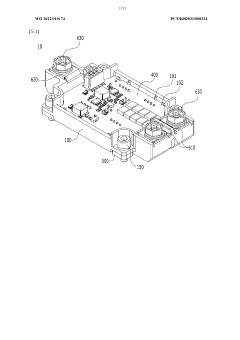
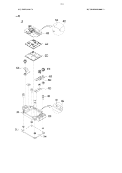
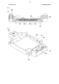
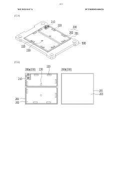
Power module
PatentWO2022010174A1
Innovation
- A power module design featuring a three-layer structure of lower and upper ceramic substrates and a PCB substrate with vertically connected electrode patterns through pins, via holes, and a metal filler to minimize current paths, enhance heat dissipation, and alleviate stress concentration by forming curvature inclined portions at the substrate edges.
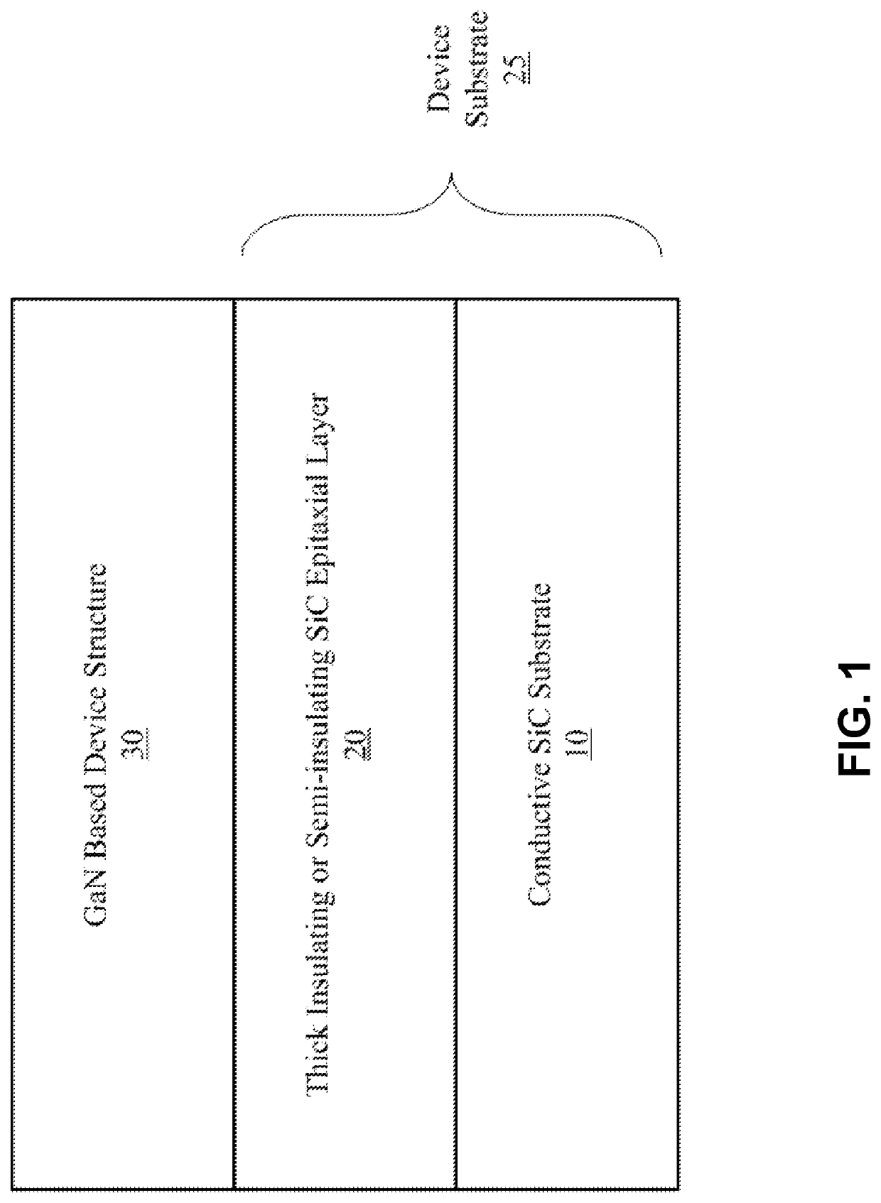
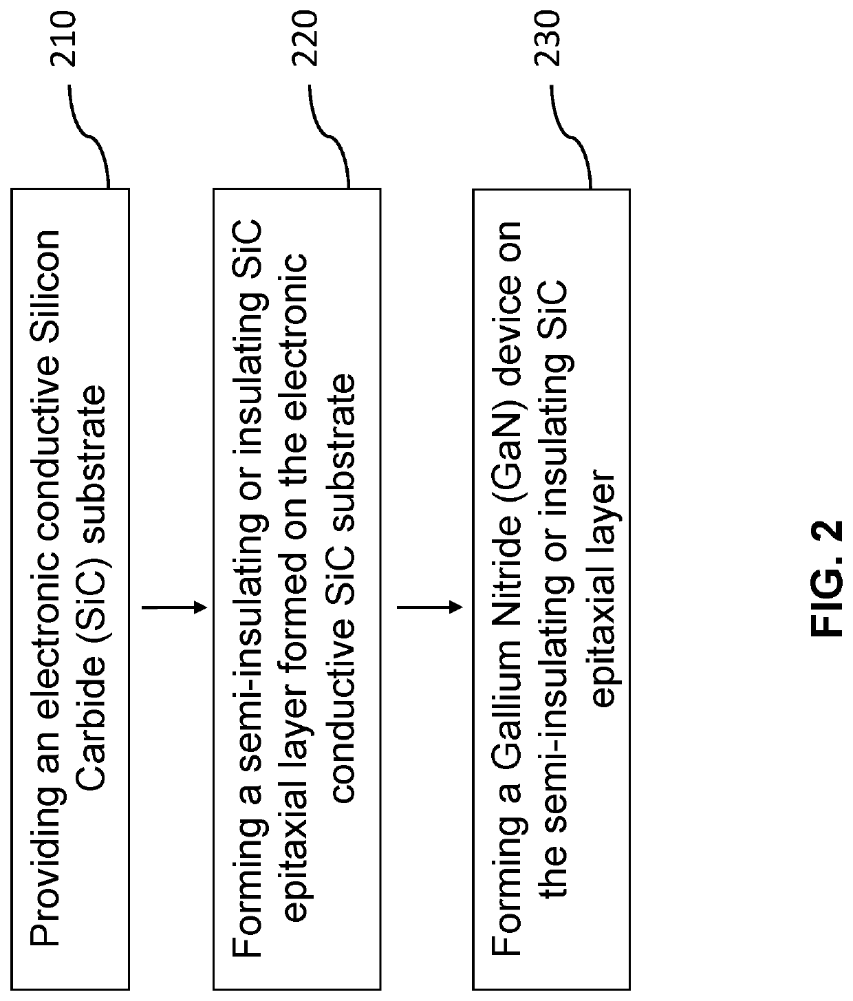
Composite substrates of conductive and insulating or semi-insulating silicon carbide for gallium nitride devices
PatentInactiveUS20200266292A1
Innovation
- A composite substrate comprising a conductive SiC substrate with an insulating/semi-insulating SiC epitaxial layer, grown using chemical vapor deposition, which facilitates the formation of GaN-based devices with improved structural quality and reduced production costs.
Thermal Management Strategies for High-Performance Power Modules
Thermal management represents a critical challenge in the design of high-performance power modules utilizing hybrid GaN HEMT and SiC solutions. The inherent high power density of these wide bandgap semiconductor devices generates significant heat during operation, necessitating advanced cooling strategies to maintain optimal performance and reliability.
The thermal conductivity differences between GaN (130 W/mK) and SiC (370 W/mK) create unique challenges in hybrid module designs. While SiC offers superior thermal performance, GaN's faster switching capabilities make the combination particularly attractive for high-frequency applications. This thermal disparity requires carefully engineered solutions to prevent hotspots and ensure uniform temperature distribution across the module.
Several thermal management approaches have demonstrated effectiveness in hybrid GaN/SiC power modules. Direct liquid cooling systems, particularly those employing microchannels beneath the semiconductor die, have shown the ability to dissipate heat fluxes exceeding 500 W/cm². These systems utilize deionized water or specialized dielectric fluids to remove heat directly from the semiconductor junction, significantly reducing thermal resistance.
Advanced thermal interface materials (TIMs) play a crucial role in hybrid module designs. Sintered silver and graphene-enhanced composites have emerged as leading options, offering thermal conductivities up to 400 W/mK while maintaining the mechanical compliance needed to accommodate the different coefficients of thermal expansion between GaN, SiC, and substrate materials.
Double-sided cooling architectures represent another promising approach, wherein heat is extracted from both the top and bottom surfaces of the power module. This configuration has demonstrated up to 40% improvement in thermal performance compared to conventional single-sided cooling in hybrid GaN/SiC implementations, particularly beneficial for high-current applications where thermal management becomes the limiting factor for power density.
Computational fluid dynamics (CFD) modeling has become essential in optimizing thermal management strategies for these complex hybrid systems. Multi-physics simulations that account for electrical, thermal, and mechanical interactions enable designers to predict hotspots and optimize cooling structures before physical prototyping, reducing development cycles and improving reliability predictions.
Recent advancements in embedded cooling technologies, where microfluidic channels are integrated directly into the module substrate, show particular promise for hybrid GaN/SiC designs. These solutions have demonstrated junction-to-ambient thermal resistances below 0.1°C/W, enabling power densities approaching 100 W/cm³ while maintaining junction temperatures below critical thresholds.
Reliability and Qualification Standards for GaN-SiC Solutions
The reliability and qualification of hybrid GaN HEMT and SiC power modules represent critical considerations for their industrial adoption. These advanced semiconductor technologies must meet stringent standards to ensure consistent performance under various operational conditions. Currently, the industry follows several established qualification frameworks, including JEDEC JEP180 for GaN devices and JEDEC JC-70.2 for SiC components, though these standards continue to evolve as the technologies mature.
Reliability testing for hybrid GaN-SiC solutions encompasses multiple dimensions beyond traditional silicon-based evaluations. Temperature cycling tests must account for the different thermal expansion coefficients between GaN and SiC materials, requiring more comprehensive thermal stress assessments. High-temperature operating life (HTOL) tests typically extend to 1000+ hours at elevated temperatures to verify long-term stability of the hybrid interfaces.
Humidity-based reliability tests present unique challenges for GaN-SiC modules due to potential moisture penetration at material interfaces. The Temperature Humidity Bias (THB) test at 85°C/85% relative humidity has become standard, with many manufacturers extending test durations beyond the typical 1000 hours to ensure robustness.
Dynamic switching reliability represents a particular concern for hybrid solutions. The fast switching capabilities of GaN HEMTs (often exceeding 200V/ns) create unique stress conditions at the GaN-SiC interface that must be thoroughly evaluated through specialized dynamic characterization methods. Short-circuit withstand capability tests must account for the different behaviors of GaN and SiC under fault conditions.
Radiation hardness testing has gained importance for aerospace and automotive applications, with hybrid GaN-SiC solutions demonstrating superior performance compared to silicon alternatives. Single Event Effect (SEE) testing has become standard for critical applications, with qualification levels typically exceeding 100 MeV·cm²/mg.
Accelerated lifetime models for hybrid solutions remain an active research area. Traditional models like Arrhenius and Coffin-Manson require modification to account for the unique degradation mechanisms at GaN-SiC interfaces. Recent research indicates that hybrid solutions may require composite reliability models that separately address GaN, SiC, and interface degradation mechanisms.
Field reliability data collection has become increasingly important, with several manufacturers implementing remote monitoring systems to gather operational data from deployed hybrid power modules. This real-world data helps refine qualification standards and improve predictive models for next-generation designs.
Unlock deeper insights with Patsnap Eureka Quick Research — get a full tech report to explore trends and direct your research. Try now!
Generate Your Research Report Instantly with AI Agent
Supercharge your innovation with Patsnap Eureka AI Agent Platform!