

Research on Chiplet Integration in Semiconductor Materials
OCT 15, 20259 MIN READ
Generate Your Research Report Instantly with AI Agent
PatSnap Eureka helps you evaluate technical feasibility & market potential.
Chiplet Technology Evolution and Integration Goals
The semiconductor industry has witnessed a paradigm shift in recent years, moving from traditional monolithic system-on-chip (SoC) designs toward more modular chiplet-based architectures. This evolution began in the early 2010s when semiconductor manufacturers faced increasing challenges with Moore's Law, as the economic and technical difficulties of shrinking transistors became more pronounced. The chiplet approach emerged as a strategic response to these limitations, allowing for the disaggregation of complex systems into smaller, specialized dies that could be manufactured separately and then integrated.
The initial chiplet implementations focused primarily on packaging multiple homogeneous dies together, as seen in AMD's first-generation EPYC processors introduced in 2017. This approach has since evolved toward heterogeneous integration, combining dies manufactured using different process nodes, technologies, and even from different vendors. This heterogeneity represents a fundamental shift in semiconductor design philosophy, prioritizing system-level optimization over monolithic integration.
The technological evolution of chiplets has been marked by significant advancements in integration methodologies. Early implementations relied on interposer-based solutions, while more recent approaches have embraced direct die-to-die connections through advanced packaging technologies such as EMIB (Embedded Multi-die Interconnect Bridge) by Intel and CoWoS (Chip-on-Wafer-on-Substrate) by TSMC. These packaging innovations have progressively reduced the communication latency and power consumption between chiplets while increasing bandwidth.
The primary goals of chiplet integration research center around several critical objectives. First, achieving cost optimization by enabling the use of optimal process nodes for different functional blocks, thereby avoiding the expense of manufacturing entire systems using cutting-edge processes. Second, improving yield management by reducing die sizes and allowing for the selective assembly of known-good dies. Third, enhancing design flexibility and reusability through standardized interfaces that facilitate the mixing and matching of chiplets from various sources.
Looking forward, the industry is moving toward establishing standardized chiplet interfaces and protocols, as evidenced by initiatives like the Universal Chiplet Interconnect Express (UCIe) consortium formed in 2022. These standards aim to create an ecosystem where chiplets from different vendors can interoperate seamlessly, potentially revolutionizing the semiconductor supply chain and business models. The ultimate vision is to establish a "chiplet marketplace" where specialized functional blocks can be sourced from various suppliers and integrated into custom solutions.
The integration goals also extend to advanced materials research, focusing on novel substrate materials, through-silicon via (TSV) technologies, and microbump innovations that can support higher connection densities, improved thermal management, and enhanced reliability for increasingly complex chiplet architectures.
The initial chiplet implementations focused primarily on packaging multiple homogeneous dies together, as seen in AMD's first-generation EPYC processors introduced in 2017. This approach has since evolved toward heterogeneous integration, combining dies manufactured using different process nodes, technologies, and even from different vendors. This heterogeneity represents a fundamental shift in semiconductor design philosophy, prioritizing system-level optimization over monolithic integration.
The technological evolution of chiplets has been marked by significant advancements in integration methodologies. Early implementations relied on interposer-based solutions, while more recent approaches have embraced direct die-to-die connections through advanced packaging technologies such as EMIB (Embedded Multi-die Interconnect Bridge) by Intel and CoWoS (Chip-on-Wafer-on-Substrate) by TSMC. These packaging innovations have progressively reduced the communication latency and power consumption between chiplets while increasing bandwidth.
The primary goals of chiplet integration research center around several critical objectives. First, achieving cost optimization by enabling the use of optimal process nodes for different functional blocks, thereby avoiding the expense of manufacturing entire systems using cutting-edge processes. Second, improving yield management by reducing die sizes and allowing for the selective assembly of known-good dies. Third, enhancing design flexibility and reusability through standardized interfaces that facilitate the mixing and matching of chiplets from various sources.
Looking forward, the industry is moving toward establishing standardized chiplet interfaces and protocols, as evidenced by initiatives like the Universal Chiplet Interconnect Express (UCIe) consortium formed in 2022. These standards aim to create an ecosystem where chiplets from different vendors can interoperate seamlessly, potentially revolutionizing the semiconductor supply chain and business models. The ultimate vision is to establish a "chiplet marketplace" where specialized functional blocks can be sourced from various suppliers and integrated into custom solutions.
The integration goals also extend to advanced materials research, focusing on novel substrate materials, through-silicon via (TSV) technologies, and microbump innovations that can support higher connection densities, improved thermal management, and enhanced reliability for increasingly complex chiplet architectures.
Market Demand Analysis for Chiplet-Based Semiconductor Solutions
The global semiconductor market is experiencing a significant shift towards chiplet-based solutions, driven by the increasing demand for more powerful, energy-efficient, and cost-effective computing systems. Market research indicates that the chiplet technology market is projected to grow at a compound annual growth rate of 40% between 2023 and 2030, reaching approximately 57 billion USD by 2030. This remarkable growth trajectory underscores the industry's recognition of chiplets as a viable solution to overcome the limitations of traditional monolithic chip designs.
The primary market drivers for chiplet-based semiconductor solutions stem from several converging factors. Data centers and cloud service providers are facing unprecedented demands for computational power while being constrained by energy consumption limits. These entities represent the largest current market segment for chiplet technology, as they seek to maximize performance per watt metrics for their server farms. The hyperscale cloud providers alone are estimated to account for 35% of the current chiplet market demand.
Consumer electronics manufacturers constitute another significant market segment, particularly in high-performance computing devices such as gaming consoles, advanced smartphones, and AI-capable devices. These applications benefit from the modular nature of chiplets, which allows for more customized solutions and faster time-to-market for new products. Industry analysts predict that consumer electronics will represent approximately 28% of the chiplet market by 2025.
Automotive and industrial applications are emerging as rapidly growing market segments for chiplet technology. Advanced driver-assistance systems (ADAS), autonomous vehicles, and industrial automation require increasingly sophisticated semiconductor solutions that can deliver high performance while meeting stringent reliability and safety standards. The automotive sector's demand for chiplet-based solutions is expected to grow by 45% annually through 2028.
From a geographical perspective, North America currently leads the chiplet market with approximately 40% share, followed by Asia-Pacific at 35% and Europe at 20%. However, the Asia-Pacific region is expected to demonstrate the fastest growth rate over the next five years due to substantial investments in semiconductor manufacturing infrastructure in countries like Taiwan, South Korea, and China.
Market analysis reveals that customers are primarily seeking chiplet solutions that address three key pain points: performance scaling beyond Moore's Law limitations, reduced development costs, and supply chain flexibility. The ability to mix and match chiplets from different process nodes and even different manufacturers represents a compelling value proposition that is driving market adoption despite the technical challenges of integration.
The primary market drivers for chiplet-based semiconductor solutions stem from several converging factors. Data centers and cloud service providers are facing unprecedented demands for computational power while being constrained by energy consumption limits. These entities represent the largest current market segment for chiplet technology, as they seek to maximize performance per watt metrics for their server farms. The hyperscale cloud providers alone are estimated to account for 35% of the current chiplet market demand.
Consumer electronics manufacturers constitute another significant market segment, particularly in high-performance computing devices such as gaming consoles, advanced smartphones, and AI-capable devices. These applications benefit from the modular nature of chiplets, which allows for more customized solutions and faster time-to-market for new products. Industry analysts predict that consumer electronics will represent approximately 28% of the chiplet market by 2025.
Automotive and industrial applications are emerging as rapidly growing market segments for chiplet technology. Advanced driver-assistance systems (ADAS), autonomous vehicles, and industrial automation require increasingly sophisticated semiconductor solutions that can deliver high performance while meeting stringent reliability and safety standards. The automotive sector's demand for chiplet-based solutions is expected to grow by 45% annually through 2028.
From a geographical perspective, North America currently leads the chiplet market with approximately 40% share, followed by Asia-Pacific at 35% and Europe at 20%. However, the Asia-Pacific region is expected to demonstrate the fastest growth rate over the next five years due to substantial investments in semiconductor manufacturing infrastructure in countries like Taiwan, South Korea, and China.
Market analysis reveals that customers are primarily seeking chiplet solutions that address three key pain points: performance scaling beyond Moore's Law limitations, reduced development costs, and supply chain flexibility. The ability to mix and match chiplets from different process nodes and even different manufacturers represents a compelling value proposition that is driving market adoption despite the technical challenges of integration.
Current Challenges in Chiplet Integration Technologies
Despite the promising advancements in chiplet technology, significant technical challenges persist that hinder widespread adoption and optimal implementation. The primary challenge lies in achieving seamless integration between different chiplets manufactured using heterogeneous processes. The interface between chiplets presents complex electrical, thermal, and mechanical issues that must be addressed simultaneously to ensure reliable operation.
Interconnect density remains a critical bottleneck in chiplet integration. As chiplet designs become more sophisticated, the number of connections between dies increases exponentially, requiring advanced packaging technologies that can support high-bandwidth, low-latency communication while maintaining signal integrity. Current micro-bump and through-silicon via (TSV) technologies struggle to meet the increasing demands for interconnect density below 35μm pitch.
Power delivery and thermal management present formidable challenges in chiplet designs. The integration of multiple dies creates thermal hotspots and uneven heat distribution across the package, potentially leading to performance degradation and reliability issues. Traditional cooling solutions become less effective as chiplet architectures become more complex, necessitating innovative thermal management approaches.
Known-good-die (KGD) testing represents another significant hurdle. Testing individual chiplets before integration is essential for maintaining yield rates, but current testing methodologies are not fully optimized for chiplet architectures. The industry lacks standardized testing protocols specifically designed for chiplets, making it difficult to ensure consistent quality across different manufacturers.
Standardization issues further complicate chiplet integration. The absence of universal standards for chiplet interfaces, protocols, and form factors limits interoperability between chiplets from different vendors. This fragmentation impedes the development of a robust chiplet ecosystem and increases design complexity for system integrators.
Manufacturing yield and cost considerations also pose significant challenges. While chiplet architecture theoretically improves yield by dividing large monolithic dies into smaller components, the additional packaging steps introduce new failure modes and yield losses. The cost benefits of chiplet integration are often offset by increased packaging complexity and testing requirements.
Material compatibility issues arise when integrating chiplets manufactured using different process nodes or substrate materials. Coefficient of thermal expansion (CTE) mismatches between materials can lead to mechanical stress, warpage, and potential reliability failures during thermal cycling. Finding compatible materials that maintain structural integrity while enabling high-performance electrical connections remains challenging.
AI and high-performance computing applications demand increasingly sophisticated chiplet solutions, pushing the boundaries of current integration technologies and highlighting the need for breakthrough innovations in interconnect, packaging, and system design methodologies.
Interconnect density remains a critical bottleneck in chiplet integration. As chiplet designs become more sophisticated, the number of connections between dies increases exponentially, requiring advanced packaging technologies that can support high-bandwidth, low-latency communication while maintaining signal integrity. Current micro-bump and through-silicon via (TSV) technologies struggle to meet the increasing demands for interconnect density below 35μm pitch.
Power delivery and thermal management present formidable challenges in chiplet designs. The integration of multiple dies creates thermal hotspots and uneven heat distribution across the package, potentially leading to performance degradation and reliability issues. Traditional cooling solutions become less effective as chiplet architectures become more complex, necessitating innovative thermal management approaches.
Known-good-die (KGD) testing represents another significant hurdle. Testing individual chiplets before integration is essential for maintaining yield rates, but current testing methodologies are not fully optimized for chiplet architectures. The industry lacks standardized testing protocols specifically designed for chiplets, making it difficult to ensure consistent quality across different manufacturers.
Standardization issues further complicate chiplet integration. The absence of universal standards for chiplet interfaces, protocols, and form factors limits interoperability between chiplets from different vendors. This fragmentation impedes the development of a robust chiplet ecosystem and increases design complexity for system integrators.
Manufacturing yield and cost considerations also pose significant challenges. While chiplet architecture theoretically improves yield by dividing large monolithic dies into smaller components, the additional packaging steps introduce new failure modes and yield losses. The cost benefits of chiplet integration are often offset by increased packaging complexity and testing requirements.
Material compatibility issues arise when integrating chiplets manufactured using different process nodes or substrate materials. Coefficient of thermal expansion (CTE) mismatches between materials can lead to mechanical stress, warpage, and potential reliability failures during thermal cycling. Finding compatible materials that maintain structural integrity while enabling high-performance electrical connections remains challenging.
AI and high-performance computing applications demand increasingly sophisticated chiplet solutions, pushing the boundaries of current integration technologies and highlighting the need for breakthrough innovations in interconnect, packaging, and system design methodologies.
Current Chiplet Integration Methodologies and Architectures
01 Advanced Packaging Technologies for Chiplet Integration
Advanced packaging technologies are crucial for chiplet integration, enabling multiple dies to be combined into a single package. These technologies include 2.5D and 3D integration methods, interposer-based solutions, and fan-out wafer-level packaging. These approaches allow for heterogeneous integration of chiplets with different functionalities, process nodes, or from different manufacturers, while maintaining high performance interconnections between the dies.- Advanced Packaging Technologies for Chiplet Integration: Advanced packaging technologies are essential for chiplet integration, enabling multiple dies to be combined into a single package. These technologies include 2.5D and 3D packaging, interposers, and through-silicon vias (TSVs) that facilitate high-density interconnections between chiplets. Such packaging approaches allow for heterogeneous integration of chiplets manufactured using different process nodes, optimizing performance while reducing manufacturing costs and improving yield rates.
- Interconnect Technologies for Chiplet-to-Chiplet Communication: Efficient communication between chiplets requires advanced interconnect technologies. These include high-bandwidth die-to-die interfaces, micro-bumps, and specialized protocols that enable low-latency, high-throughput data transfer between chiplets. The interconnect technologies must address challenges such as signal integrity, power delivery, and thermal management while supporting the increasing bandwidth demands of modern computing applications.
- Thermal Management Solutions for Chiplet Designs: Thermal management is critical in chiplet integration due to the high power density and potential hotspots created by stacking multiple dies. Solutions include integrated heat spreaders, thermal interface materials, and advanced cooling techniques such as liquid cooling or microfluidic channels. Effective thermal management ensures reliable operation and prevents performance degradation due to thermal throttling in chiplet-based systems.
- Design and Testing Methodologies for Chiplet-Based Systems: Specialized design and testing methodologies are required for chiplet-based systems to ensure functionality and reliability. These include design-for-test approaches, known-good-die testing, and system-level verification techniques that address the unique challenges of multi-die integration. Advanced EDA tools support chiplet-based design flows, enabling efficient partitioning, placement, and routing across multiple dies while optimizing for performance, power, and area constraints.
- Standardization and Interoperability Frameworks for Chiplets: Standardization efforts are emerging to enable interoperability between chiplets from different vendors. These frameworks define common interfaces, protocols, and physical specifications that allow chiplets to be mixed and matched in a modular fashion. Industry consortia are developing open standards for chiplet interfaces, enabling a more diverse ecosystem of chiplet providers and accelerating adoption of chiplet-based design approaches across the semiconductor industry.
02 Interconnect Technologies for Chiplet-to-Chiplet Communication
Efficient communication between chiplets requires specialized interconnect technologies. These include high-bandwidth, low-latency interfaces such as advanced through-silicon vias (TSVs), micro-bumps, and die-to-die bridges. Novel interconnect architectures optimize data transfer between chiplets while minimizing power consumption and signal degradation, which is essential for maintaining system performance in multi-chiplet designs.Expand Specific Solutions03 Thermal Management Solutions for Chiplet Designs
Thermal management is a critical challenge in chiplet integration due to high power densities and potential hotspots at chiplet interfaces. Solutions include advanced thermal interface materials, integrated heat spreaders, microchannel cooling systems, and thermal-aware placement of chiplets. Effective thermal management strategies ensure reliable operation and prevent performance degradation in multi-chiplet packages.Expand Specific Solutions04 Design and Testing Methodologies for Chiplet-Based Systems
Specialized design and testing methodologies are required for chiplet-based systems. These include design automation tools for chiplet placement and routing, pre-silicon validation techniques, and post-integration testing strategies. Known-good-die testing before integration and built-in self-test capabilities help ensure functionality and reliability of the final integrated system, addressing the unique challenges of multi-die architectures.Expand Specific Solutions05 Standardization and Interoperability Frameworks for Chiplets
Standardization efforts are emerging to facilitate chiplet interoperability across different vendors and technologies. These frameworks include standardized interfaces, protocols, and physical specifications that enable chiplets from various sources to work together seamlessly. Industry consortia are developing open chiplet interfaces and ecosystem approaches to promote modular design methodologies and reduce integration challenges in heterogeneous chiplet systems.Expand Specific Solutions
Key Industry Players in Chiplet Ecosystem
The chiplet integration market in semiconductor materials is currently in a growth phase, characterized by increasing adoption across the industry. The global market size is expanding rapidly, driven by demand for advanced computing solutions and heterogeneous integration. From a technical maturity perspective, industry leaders like TSMC, Intel, and AMD are at the forefront, having developed sophisticated chiplet architectures and integration technologies. Samsung Electronics and Micron Technology are advancing memory-focused chiplet solutions, while SMIC and SK hynix are making significant investments in this space. Research institutions like Imec are collaborating with these companies to overcome technical challenges in interconnect density and thermal management. The ecosystem is evolving with specialized players like STATS ChipPAC providing advanced packaging solutions critical for chiplet integration.
Taiwan Semiconductor Manufacturing Co., Ltd.
Technical Solution: TSMC has developed comprehensive chiplet integration technologies through their 3DFabric platform, which encompasses both frontend and backend integration solutions. Their System on Integrated Chips (SoIC) technology provides chip-on-wafer and wafer-on-wafer bonding with ultra-high-density interconnects at less than 10μm pitch, enabling true 3D integration. TSMC's Integrated Fan-Out (InFO) and Chip on Wafer on Substrate (CoWoS) technologies provide advanced packaging options for chiplet integration with varying levels of performance, density, and cost. Their latest CoWoS-R technology supports reticle-size interposers exceeding 2500mm², allowing integration of multiple large chiplets in a single package. TSMC has also developed their LIPINCON (Low-voltage-In-Package-INterCONnect) die-to-die interface, supporting bandwidths up to 8GT/s with energy efficiency below 0.3pJ/bit, addressing both performance and power requirements for chiplet designs.
Strengths: As the world's leading semiconductor foundry, TSMC offers unmatched process technology integration with their packaging solutions, providing a complete ecosystem for chiplet development. Their manufacturing scale enables cost-effective deployment of advanced packaging technologies. Weaknesses: Their most advanced integration technologies come at premium pricing, potentially limiting adoption to high-value applications, and customers must navigate complex design rules and manufacturing constraints.
Samsung Electronics Co., Ltd.
Technical Solution: Samsung's chiplet integration strategy centers on their I-Cube (Interposer-Cube) technology, which uses silicon interposers to connect multiple dies with high-bandwidth, short-reach interconnects. Their latest I-Cube4 technology supports larger interposer sizes and finer interconnect pitches, enabling more complex multi-die integration. Samsung has also developed their X-Cube technology for true 3D stacking using hybrid bonding with TSVs, achieving vertical interconnect pitches below 10μm. This enables logic-on-logic stacking with significantly higher interconnect density than traditional package-level integration. Samsung's Advanced Package-on-Package (PoP) technology extends chiplet concepts to memory integration, particularly for mobile applications, stacking HBM or LPDDR memory directly on logic dies. Their heterogeneous integration approach supports mixing dies from different process nodes, allowing optimization of each function on its ideal manufacturing technology while maintaining high-bandwidth connections between components.
Strengths: Samsung's vertical integration as both a foundry and device manufacturer gives them unique insights into system-level optimization of chiplet designs. Their memory expertise enables particularly effective integration of logic and memory components. Weaknesses: Their chiplet ecosystem is less mature than some competitors, with fewer public implementations in high-volume products, and their proprietary interconnect standards may limit broader industry adoption.
Core Patents and Innovations in Chiplet Integration
Processes, articles and apparatus that incorporate semiconductor switches and drive circuitry on compound semiconductor chiplets
PatentInactiveUS20220077223A1
Innovation
- The fabrication process involves forming chiplets with a first semiconductor material optimized for specific functionalities, such as LEDs, and combining them with a second semiconductor material for thin film transistors, which are then transferred to a target substrate using various techniques like pick and place machinery or selective laser release, enabling the integration of both functionalities in a single structure.


Semiconductor packaging structure and preparation method thereof
PatentActiveCN118431177B
Innovation
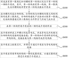
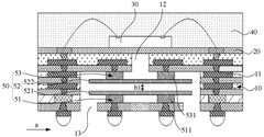
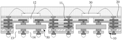
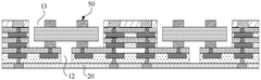
- A semiconductor packaging structure is designed, including a wiring structure with conductive lines, a dielectric layer, a chip and a cooling structure. The cooling structure is electrically connected to the conductive lines. After being energized, it vibrates to form an airflow pressure difference and communicates with the outside air through the first heat dissipation hole. An airflow pressure difference is formed to improve heat dissipation performance, and the chip is packaged through the dielectric layer and plastic sealing layer to avoid external power supply interference.
Supply Chain Considerations for Chiplet Manufacturing
The global chiplet supply chain represents a complex ecosystem that requires careful orchestration of multiple specialized vendors and manufacturing processes. Unlike traditional monolithic chip production, chiplet-based designs involve the integration of multiple smaller dies, necessitating a more distributed and specialized manufacturing approach. This fragmentation creates both opportunities and challenges for semiconductor companies adopting chiplet architectures.
Material sourcing for chiplet manufacturing presents unique challenges compared to traditional semiconductor production. The diverse nature of chiplet designs often requires specialized substrate materials with precise thermal and electrical properties to facilitate high-bandwidth die-to-die interconnects. Companies must establish reliable supply channels for advanced packaging materials, including organic substrates, silicon interposers, and specialized bonding materials that can withstand the thermal and mechanical stresses of multi-die integration.
Manufacturing capacity allocation represents another critical consideration in the chiplet supply chain. With different chiplets potentially manufactured using different process nodes at various foundries, companies must carefully coordinate production schedules and capacity reservations across multiple manufacturing partners. This multi-vendor approach can provide resilience against regional disruptions but requires sophisticated supply chain management systems to maintain production continuity.
Quality control and testing procedures become significantly more complex in chiplet manufacturing. Each individual chiplet must undergo rigorous testing before integration, and additional testing is required after assembly to verify inter-chiplet communication. This multi-stage testing approach necessitates specialized equipment and expertise, creating potential bottlenecks in the supply chain that must be carefully managed.
Inventory management strategies must evolve to accommodate the modular nature of chiplet designs. Companies may need to maintain inventories of standardized chiplets that can be rapidly integrated into various products, balancing the benefits of component reuse against inventory carrying costs. This approach requires sophisticated demand forecasting to prevent shortages or excess inventory of specific chiplet components.
Geopolitical considerations increasingly impact chiplet supply chains, with national security concerns and export controls affecting the movement of advanced semiconductor technologies. Companies must navigate these restrictions while maintaining access to critical manufacturing capabilities, potentially through diversified manufacturing footprints or strategic partnerships in multiple regions.
Material sourcing for chiplet manufacturing presents unique challenges compared to traditional semiconductor production. The diverse nature of chiplet designs often requires specialized substrate materials with precise thermal and electrical properties to facilitate high-bandwidth die-to-die interconnects. Companies must establish reliable supply channels for advanced packaging materials, including organic substrates, silicon interposers, and specialized bonding materials that can withstand the thermal and mechanical stresses of multi-die integration.
Manufacturing capacity allocation represents another critical consideration in the chiplet supply chain. With different chiplets potentially manufactured using different process nodes at various foundries, companies must carefully coordinate production schedules and capacity reservations across multiple manufacturing partners. This multi-vendor approach can provide resilience against regional disruptions but requires sophisticated supply chain management systems to maintain production continuity.
Quality control and testing procedures become significantly more complex in chiplet manufacturing. Each individual chiplet must undergo rigorous testing before integration, and additional testing is required after assembly to verify inter-chiplet communication. This multi-stage testing approach necessitates specialized equipment and expertise, creating potential bottlenecks in the supply chain that must be carefully managed.
Inventory management strategies must evolve to accommodate the modular nature of chiplet designs. Companies may need to maintain inventories of standardized chiplets that can be rapidly integrated into various products, balancing the benefits of component reuse against inventory carrying costs. This approach requires sophisticated demand forecasting to prevent shortages or excess inventory of specific chiplet components.
Geopolitical considerations increasingly impact chiplet supply chains, with national security concerns and export controls affecting the movement of advanced semiconductor technologies. Companies must navigate these restrictions while maintaining access to critical manufacturing capabilities, potentially through diversified manufacturing footprints or strategic partnerships in multiple regions.
Thermal Management Strategies for Multi-Chiplet Systems
Thermal management has emerged as a critical challenge in multi-chiplet systems due to the increased power density and heterogeneous integration of different functional blocks. As chiplets are placed in close proximity, heat dissipation becomes more complex compared to traditional monolithic designs. Current thermal management strategies employ a multi-layered approach combining both passive and active cooling techniques to maintain optimal operating temperatures.
Advanced thermal interface materials (TIMs) play a crucial role in chiplet integration by facilitating efficient heat transfer between components. Recent developments in TIMs include metal-based composites with thermal conductivities exceeding 20 W/m·K, significantly outperforming traditional polymer-based materials. Graphene and carbon nanotube-enhanced TIMs have demonstrated promising results in laboratory settings, potentially reducing thermal resistance by up to 30% compared to conventional solutions.
Microfluidic cooling channels integrated directly into interposer substrates represent another innovative approach for multi-chiplet thermal management. These channels allow coolant circulation in close proximity to heat-generating components, enabling targeted cooling of hotspots. Implementation challenges include miniaturization of fluid channels, prevention of leakage, and integration with existing packaging technologies. Despite these challenges, microfluidic cooling has demonstrated heat flux dissipation capabilities exceeding 500 W/cm² in experimental setups.
Three-dimensional heat spreading architectures utilizing through-silicon vias (TSVs) and thermal TSVs (T-TSVs) provide vertical thermal pathways in stacked chiplet configurations. These structures can reduce junction-to-ambient thermal resistance by up to 40% compared to conventional cooling methods. The effectiveness of T-TSVs depends on their diameter, density, and placement relative to hotspots within the chiplet stack.
Dynamic thermal management (DTM) strategies incorporate real-time temperature monitoring and adaptive control mechanisms. Advanced DTM systems employ machine learning algorithms to predict thermal behavior and preemptively adjust workloads across chiplets. This approach has shown to reduce peak temperatures by 15-20% while maintaining performance targets in high-performance computing applications.
Emerging technologies such as phase-change materials (PCMs) embedded within chiplet packages offer promising thermal buffering capabilities. These materials absorb heat during phase transition, effectively dampening temperature fluctuations during burst workloads. Silicon-integrated PCMs with melting points between 60-90°C have demonstrated the ability to reduce thermal cycling amplitude by up to 25%, potentially extending device reliability and lifetime.
Advanced thermal interface materials (TIMs) play a crucial role in chiplet integration by facilitating efficient heat transfer between components. Recent developments in TIMs include metal-based composites with thermal conductivities exceeding 20 W/m·K, significantly outperforming traditional polymer-based materials. Graphene and carbon nanotube-enhanced TIMs have demonstrated promising results in laboratory settings, potentially reducing thermal resistance by up to 30% compared to conventional solutions.
Microfluidic cooling channels integrated directly into interposer substrates represent another innovative approach for multi-chiplet thermal management. These channels allow coolant circulation in close proximity to heat-generating components, enabling targeted cooling of hotspots. Implementation challenges include miniaturization of fluid channels, prevention of leakage, and integration with existing packaging technologies. Despite these challenges, microfluidic cooling has demonstrated heat flux dissipation capabilities exceeding 500 W/cm² in experimental setups.
Three-dimensional heat spreading architectures utilizing through-silicon vias (TSVs) and thermal TSVs (T-TSVs) provide vertical thermal pathways in stacked chiplet configurations. These structures can reduce junction-to-ambient thermal resistance by up to 40% compared to conventional cooling methods. The effectiveness of T-TSVs depends on their diameter, density, and placement relative to hotspots within the chiplet stack.
Dynamic thermal management (DTM) strategies incorporate real-time temperature monitoring and adaptive control mechanisms. Advanced DTM systems employ machine learning algorithms to predict thermal behavior and preemptively adjust workloads across chiplets. This approach has shown to reduce peak temperatures by 15-20% while maintaining performance targets in high-performance computing applications.
Emerging technologies such as phase-change materials (PCMs) embedded within chiplet packages offer promising thermal buffering capabilities. These materials absorb heat during phase transition, effectively dampening temperature fluctuations during burst workloads. Silicon-integrated PCMs with melting points between 60-90°C have demonstrated the ability to reduce thermal cycling amplitude by up to 25%, potentially extending device reliability and lifetime.
Unlock deeper insights with PatSnap Eureka Quick Research — get a full tech report to explore trends and direct your research. Try now!
Generate Your Research Report Instantly with AI Agent
Supercharge your innovation with PatSnap Eureka AI Agent Platform!