Substrate Choices And Thermal Conductivity Considerations
AUG 27, 20259 MIN READ
Generate Your Research Report Instantly with AI Agent
Patsnap Eureka helps you evaluate technical feasibility & market potential.
Substrate Technology Background and Objectives
Substrate technology has evolved significantly over the past several decades, transitioning from simple mechanical support structures to sophisticated engineered materials that actively contribute to device performance. The journey began with basic ceramic and glass substrates in the 1960s, progressing through various materials including polymers, metals, and advanced composites. Each evolution has been driven by increasing demands for thermal management, electrical performance, and mechanical reliability in electronic systems.
Thermal conductivity has emerged as a critical parameter in substrate selection, particularly as power densities in electronic devices continue to rise exponentially. Historical data shows that power densities in semiconductor devices have increased by approximately 30% annually over the past decade, creating unprecedented thermal management challenges. This trend necessitates substrates with superior thermal properties to prevent performance degradation and ensure device longevity.
The current substrate landscape encompasses a diverse range of materials, from traditional FR-4 with thermal conductivity of 0.3 W/mK to advanced ceramic substrates exceeding 170 W/mK. Aluminum nitride (AlN), silicon carbide (SiC), and diamond-based composites represent the cutting edge of thermally conductive substrate materials, offering solutions for the most demanding applications in power electronics, RF/microwave systems, and high-performance computing.
Industry projections indicate that the global market for thermally conductive substrates will reach $3.2 billion by 2026, growing at a CAGR of 6.8%. This growth is primarily driven by expanding applications in automotive electronics, 5G infrastructure, and data centers, where thermal management is increasingly becoming a limiting factor in system design and performance.
The primary objective of substrate technology development is to achieve an optimal balance between thermal conductivity, electrical properties, mechanical strength, and cost-effectiveness. Current research aims to develop substrates that can efficiently dissipate heat from increasingly dense and powerful electronic components while maintaining electrical isolation and mechanical integrity under various environmental conditions.
Emerging trends in substrate technology include the development of heterogeneous substrate structures with localized thermal management capabilities, integration of phase-change materials for transient thermal control, and exploration of two-dimensional materials like graphene for next-generation thermal interfaces. These innovations seek to address the fundamental limitations of conventional materials while enabling new device architectures and applications.
The convergence of material science, thermal engineering, and electronic design automation is creating unprecedented opportunities for substrate technology advancement. By understanding the historical context and current trajectory of substrate materials, we can better anticipate future developments and align research efforts with industry needs and technological possibilities.
Market Analysis for High Thermal Conductivity Materials
The global market for high thermal conductivity materials is experiencing robust growth, driven primarily by increasing demand in electronics, automotive, aerospace, and energy sectors. As of 2023, the market size is valued at approximately 12.5 billion USD with a compound annual growth rate (CAGR) of 8.3% projected through 2030. This growth trajectory is significantly influenced by the miniaturization trend in electronics and the growing thermal management challenges in high-performance computing systems.
Consumer electronics represents the largest application segment, accounting for nearly 35% of the total market share. The proliferation of smartphones, tablets, and wearable devices has intensified the need for efficient heat dissipation in compact form factors. Additionally, the automotive industry is rapidly emerging as a key consumer of these materials, particularly with the expansion of electric vehicles where battery thermal management is critical for performance and safety.
Regionally, Asia-Pacific dominates the market with approximately 45% share, attributed to the concentration of electronics manufacturing in countries like China, Japan, South Korea, and Taiwan. North America follows with 28% market share, driven by aerospace, defense, and advanced computing applications. Europe accounts for 20% of the market, with strong demand from automotive and industrial sectors.
Material-wise, the market is segmented into metals (copper, aluminum), ceramics (aluminum nitride, silicon carbide), carbon-based materials (graphite, graphene), and polymeric composites. Notably, carbon-based materials are witnessing the fastest growth rate at 12.7% annually, owing to their superior thermal conductivity properties and decreasing production costs.
Key market drivers include the growing adoption of 5G technology, which requires enhanced thermal management solutions for base stations and devices. The data center industry is another significant driver, with increasing power densities necessitating more efficient cooling solutions. Additionally, the transition toward renewable energy systems has created demand for thermal interface materials in solar inverters and wind power electronics.
Market challenges include the high cost of advanced materials like synthetic diamond and graphene, which limits widespread adoption. Supply chain vulnerabilities, particularly for rare earth elements used in certain high-performance ceramics, present another constraint. Environmental regulations regarding the production and disposal of certain materials also impact market dynamics.
Current Substrate Technologies and Thermal Challenges
The semiconductor industry currently employs various substrate materials, each with distinct thermal properties that significantly impact device performance. Silicon (Si) remains the dominant substrate material due to its cost-effectiveness, established manufacturing ecosystem, and reasonable thermal conductivity of approximately 150 W/m·K. However, as power densities continue to increase in modern electronic devices, silicon's thermal limitations have become increasingly apparent, particularly in high-power applications.
Silicon carbide (SiC) has emerged as a prominent alternative with superior thermal conductivity ranging from 300-490 W/m·K, enabling it to dissipate heat more efficiently than silicon. This property, combined with its wide bandgap characteristics, makes SiC particularly valuable for power electronics and high-temperature applications. Despite these advantages, SiC substrates face challenges related to higher manufacturing costs and defect densities compared to silicon.
Gallium nitride (GaN) represents another significant substrate technology, often grown on silicon, silicon carbide, or sapphire. While bulk GaN offers excellent thermal conductivity (approximately 230 W/m·K), the thermal performance of GaN-on-Si or GaN-on-SiC is limited by interface thermal resistance and substrate properties. The heterogeneous integration creates thermal bottlenecks that require innovative solutions.
Diamond stands as the ultimate thermal conductor with exceptional thermal conductivity exceeding 2000 W/m·K. Recent advances in chemical vapor deposition (CVD) diamond growth have enabled its integration as a heat spreader or substrate material. However, widespread adoption remains constrained by prohibitive costs, limited wafer sizes, and integration challenges with semiconductor processing.
Aluminum nitride (AlN) offers another alternative with thermal conductivity around 170-285 W/m·K and excellent electrical insulation properties. Its compatibility with semiconductor processing makes it valuable for specialized applications, though cost factors limit broader implementation.
The primary thermal challenges facing current substrate technologies include thermal boundary resistance at material interfaces, which creates bottlenecks for heat dissipation. As devices scale down, the increasing power density exacerbates thermal management issues, with hotspots becoming more concentrated and difficult to mitigate. Additionally, the thermal expansion coefficient mismatch between different materials in heterogeneous integration leads to mechanical stress and potential reliability concerns.
Advanced packaging technologies like 3D integration further complicate thermal management by stacking multiple active layers with limited pathways for heat extraction. The industry is actively exploring solutions including novel thermal interface materials, embedded cooling channels, and advanced thermal simulation tools to address these challenges while maintaining performance and reliability requirements.
Existing Substrate Material Solutions
01 High thermal conductivity substrate materials
Various materials with high thermal conductivity properties are used as substrates in electronic and thermal management applications. These materials include ceramics, metal composites, and specialized polymers that efficiently dissipate heat from components. The high thermal conductivity of these substrates helps prevent overheating of electronic devices, improves device performance, and extends the lifespan of components by maintaining optimal operating temperatures.- High thermal conductivity substrate materials: Various materials with high thermal conductivity properties are used as substrates in electronic and thermal management applications. These materials include ceramics, metal composites, and specialized polymers that efficiently dissipate heat. The high thermal conductivity of these substrates helps prevent overheating of components, improves device performance, and extends the lifespan of electronic systems by maintaining optimal operating temperatures.
- Thermal conductivity measurement methods for substrates: Various techniques and apparatus are employed to measure the thermal conductivity of substrate materials. These methods include thermal transient testing, laser flash analysis, and steady-state heat flow measurements. Accurate measurement of thermal conductivity is crucial for material selection in applications where heat management is critical, enabling engineers to design systems with optimal thermal performance.
- Substrate thermal interface materials: Thermal interface materials are applied between substrates and heat-generating components to improve thermal conductivity across contact surfaces. These materials include thermal greases, phase change materials, and thermally conductive adhesives that fill microscopic air gaps and enhance heat transfer. By reducing thermal resistance at interfaces, these materials significantly improve overall thermal management in electronic assemblies and other heat-sensitive applications.
- Layered and composite substrate structures for thermal management: Multi-layered and composite substrate structures are designed to optimize thermal conductivity in specific directions or applications. These engineered substrates combine different materials with complementary thermal properties to achieve targeted heat dissipation. The layered approach allows for customization of thermal pathways, enabling efficient heat transfer from hot spots to heat sinks or cooling systems while maintaining structural integrity and other required properties.
- Substrate cooling systems and heat dissipation structures: Various cooling systems and heat dissipation structures are integrated with or attached to substrates to enhance thermal management. These include microchannels for liquid cooling, heat pipes, vapor chambers, and specialized fin structures. Such systems actively or passively remove heat from substrates, maintaining optimal operating temperatures for electronic components and other heat-generating devices, particularly in high-power applications where conventional thermal management approaches are insufficient.
02 Thermal conductivity measurement methods for substrates
Various techniques and apparatus are employed to measure the thermal conductivity of substrate materials. These methods include transient plane source techniques, laser flash analysis, and thermal impedance measurements. Accurate measurement of thermal conductivity is crucial for material selection in applications where heat management is critical, allowing engineers to properly design thermal management systems and predict the performance of materials under various thermal conditions.Expand Specific Solutions03 Substrate thermal interface materials
Thermal interface materials are applied between substrates and heat-generating components to improve thermal conductivity across contact surfaces. These materials include thermal greases, phase change materials, and thermally conductive adhesives that fill microscopic air gaps between surfaces. By enhancing the thermal contact between components and heat sinks or other cooling structures, these materials significantly improve overall heat dissipation efficiency in electronic assemblies.Expand Specific Solutions04 Layered and composite substrate structures for thermal management
Multi-layered and composite substrate structures are designed to optimize thermal conductivity in specific directions or applications. These structures may combine materials with different thermal properties to create substrates with tailored thermal management capabilities. By strategically arranging layers of different materials, engineers can direct heat flow paths, create thermal barriers where needed, or enhance heat spreading in critical areas, resulting in more efficient thermal management solutions.Expand Specific Solutions05 Substrate cooling systems and heat dissipation structures
Various cooling systems and structures are integrated with substrates to enhance heat dissipation. These include microchannels for liquid cooling, embedded heat pipes, fin structures, and specialized thermal vias. These features are designed to efficiently transfer heat away from critical components through the substrate material. Advanced cooling solutions can significantly improve the thermal performance of electronic devices, allowing for higher power densities and more compact designs.Expand Specific Solutions
Leading Manufacturers and Research Institutions
The substrate choices and thermal conductivity market is in a growth phase, with increasing demand driven by electronics miniaturization and thermal management challenges. The market is estimated to reach significant value as thermal solutions become critical for advanced electronics. Technologically, the field shows varying maturity levels across applications, with companies demonstrating different specializations. Leading players like Sumitomo Electric, Kyocera, and NGK Insulators offer advanced ceramic substrates, while AT&S focuses on high-end PCB technologies. Research institutions such as AIST and Xiamen University are advancing fundamental materials science, while semiconductor manufacturers like Renesas and Qualcomm drive application-specific innovations in thermal management solutions.
Sumitomo Electric Industries Ltd.
Technical Solution: Sumitomo Electric has pioneered diamond-based substrate technology for thermal management applications. Their CVD (Chemical Vapor Deposition) synthetic diamond substrates achieve remarkable thermal conductivity values of 1,000-2,000 W/m·K, approximately 5 times higher than copper. The company utilizes a proprietary microwave plasma CVD process to grow polycrystalline diamond films with controlled grain structure and minimal defects. For semiconductor packaging applications, Sumitomo has developed composite substrates combining diamond with metals like copper and aluminum, creating direct bonded structures that efficiently transfer heat from devices to cooling systems. Their "SUMICRYSTAL" diamond heat spreaders are particularly effective for high-power RF and laser applications, where they've demonstrated temperature reductions of 30-50% compared to conventional materials, significantly improving device reliability and performance.
Strengths: Exceptional thermal conductivity exceeding all conventional materials; low thermal expansion coefficient matching semiconductor materials; chemical inertness and stability at high temperatures. Weaknesses: Very high production costs limiting widespread adoption; challenges in creating large-area substrates; difficulty in metallization and integration with standard packaging processes.
Kyocera Corp.
Technical Solution: Kyocera has developed a comprehensive portfolio of ceramic substrate solutions optimized for thermal conductivity. Their aluminum nitride (AlN) substrates achieve thermal conductivity values of 170-230 W/m·K through proprietary sintering additives and controlled grain boundary engineering. For cost-sensitive applications, Kyocera offers aluminum oxide (Al2O3) substrates with enhanced thermal properties (25-40 W/m·K) achieved through particle size optimization and high-density sintering. The company's "Silicon Nitride AMB" technology bonds active metal layers directly to silicon nitride ceramics, creating robust substrates for harsh environments with thermal cycling resistance superior to conventional DBC substrates. Kyocera has also pioneered multilayer ceramic substrates with embedded thermal vias and channels, allowing three-dimensional heat flow paths that can reduce thermal resistance by up to 40% compared to conventional planar designs.
Strengths: Wide range of material options allowing cost-performance optimization; excellent mechanical strength and reliability; established manufacturing infrastructure enabling consistent quality and volume production. Weaknesses: Lower maximum thermal conductivity than diamond-based solutions; some ceramic formulations have higher dielectric losses at high frequencies; potential for thermal stress at material interfaces during extreme temperature cycling.
Key Thermal Conductivity Enhancement Technologies
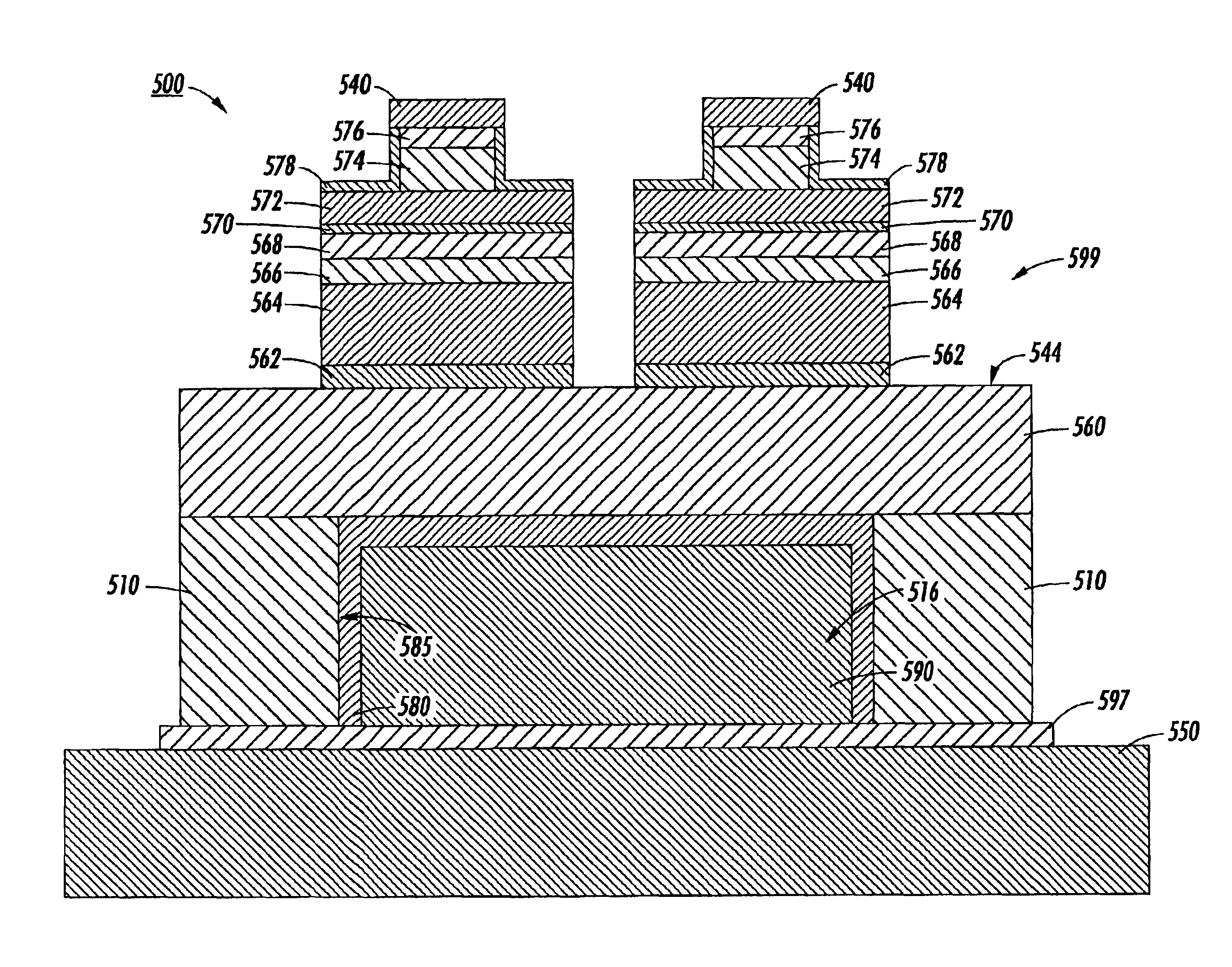
Substrate for element-mounted device
PatentInactiveEP1154476B1
Innovation
- A substrate with a high thermal conductivity material layer, such as diamond, featuring a flow path or groove for coolant passage adjacent to the interface with a base material, enhancing heat dissipation by minimizing thermal resistance and maintaining element temperature within a safe range.


Substrates having increased thermal conductivity for semiconductor structures
PatentInactiveUS6744072B2
Innovation
- Creating substrates with enhanced thermal conductivity by forming cavities in the substrate and filling them with materials like copper, which improves heat dissipation and reduces thermal resistance, thereby lowering device temperatures and minimizing thermal cross-talk.

Environmental Impact of Substrate Materials
The environmental impact of substrate materials in electronic and thermal management applications has become increasingly significant as industries strive for sustainability alongside performance. Silicon, the traditional substrate material, presents considerable environmental challenges throughout its lifecycle. The extraction of silicon requires extensive mining operations that contribute to habitat destruction, while its purification process is energy-intensive, consuming approximately 200 kWh per kilogram of processed silicon. This energy demand translates to substantial carbon emissions, estimated at 54-70 kg CO2 equivalent per kilogram of electronic-grade silicon.
Alternative substrate materials offer varying environmental profiles. Aluminum nitride (AlN), while providing excellent thermal conductivity, requires high-temperature synthesis processes that consume significant energy. However, its extended operational lifespan and recyclability partially offset these initial environmental costs. Ceramic substrates generally demonstrate lower environmental impacts during production compared to silicon but may present challenges in end-of-life management due to limited recycling infrastructure.
Emerging substrate materials such as graphene and diamond-based substrates show promising environmental characteristics. Synthetic diamond substrates, despite their energy-intensive production, offer exceptional longevity and thermal performance that may justify their initial environmental footprint through extended product lifecycles. Graphene-based substrates potentially represent the most environmentally favorable option, with lower production energy requirements and excellent thermal properties, though commercial-scale production remains challenging.
The manufacturing processes for substrate materials contribute significantly to their overall environmental impact. Chemical vapor deposition (CVD) techniques used for diamond and some ceramic substrates generate hazardous byproducts requiring specialized disposal. Water usage is another critical factor, with traditional silicon wafer production consuming approximately 2,000-4,000 gallons of ultra-pure water per square meter of substrate material.
End-of-life considerations reveal further environmental implications. The composite nature of many advanced substrate materials complicates recycling efforts, often resulting in downcycling rather than true recycling. Silicon carbide (SiC) substrates demonstrate better recyclability profiles than gallium nitride (GaN) substrates, which contain materials classified as critical raw materials with supply chain vulnerabilities.
Regulatory frameworks increasingly influence substrate material selection, with the European Union's Restriction of Hazardous Substances (RoHS) directive and the Waste Electrical and Electronic Equipment (WEEE) directive imposing strict requirements on material composition and recyclability. These regulations are driving innovation toward more environmentally benign substrate materials that maintain or enhance thermal conductivity performance.
Cost-Performance Analysis of Substrate Options
When evaluating substrate materials for electronic applications, cost-performance analysis becomes a critical decision-making factor. Different substrate materials offer varying thermal conductivity properties at different price points, creating a spectrum of options for manufacturers to consider based on their specific requirements and budget constraints.
Aluminum substrates represent an excellent middle-ground option, offering thermal conductivity values typically ranging from 150-200 W/mK at a moderate cost point. This makes aluminum-based solutions particularly attractive for consumer electronics and automotive applications where cost sensitivity exists alongside thermal management needs. The cost-effectiveness ratio of aluminum substrates has contributed to their widespread adoption across multiple industries.
Copper substrates, while approximately 1.5-2 times more expensive than aluminum alternatives, deliver superior thermal conductivity (380-400 W/mK). This premium performance justifies the higher investment in applications where thermal management is critical, such as high-power LED systems, power electronics, and telecommunications infrastructure. Market analysis indicates that despite higher initial costs, copper substrates often demonstrate better long-term value through extended device lifespans and improved reliability metrics.
Ceramic substrates, particularly aluminum nitride (AlN) and aluminum oxide (Al₂O₃), present interesting cost-performance considerations. AlN offers exceptional thermal conductivity (170-230 W/mK) but at significantly higher costs—often 3-5 times that of aluminum substrates. Al₂O₃, while more affordable, provides modest thermal performance (20-30 W/mK). These ceramic options are typically reserved for specialized applications where electrical isolation properties are as important as thermal management.
Recent market trends show increasing interest in composite substrate materials that blend cost-effective carriers with high-performance thermal interfaces. These engineered solutions aim to optimize the cost-performance ratio by strategically employing expensive materials only where thermally necessary. For instance, copper-clad aluminum substrates provide enhanced thermal performance at approximately 30-40% lower cost than pure copper solutions.
Manufacturing scale significantly impacts substrate economics. Volume production can reduce unit costs by 25-40% for most substrate types, though this effect is less pronounced with exotic materials like diamond-based substrates. Additionally, regional manufacturing capabilities influence pricing, with Asian suppliers typically offering more competitive pricing but potentially longer supply chains compared to domestic options.
Unlock deeper insights with Patsnap Eureka Quick Research — get a full tech report to explore trends and direct your research. Try now!
Generate Your Research Report Instantly with AI Agent
Supercharge your innovation with Patsnap Eureka AI Agent Platform!