Transparent Transistors: Market Trends and Opportunities
OCT 21, 202510 MIN READ
Generate Your Research Report Instantly with AI Agent
Patsnap Eureka helps you evaluate technical feasibility & market potential.
Transparent Transistor Technology Evolution and Objectives
Transparent transistors have emerged as a revolutionary technology in the electronics industry, evolving from early experimental concepts to commercially viable components over the past two decades. The journey began in the early 2000s with the development of amorphous oxide semiconductors, particularly indium gallium zinc oxide (IGZO), which demonstrated unprecedented combinations of optical transparency and electrical performance. This breakthrough marked a significant departure from traditional silicon-based transistors that dominated the industry for decades.
The evolution of transparent transistor technology has been characterized by continuous improvements in material science, fabrication techniques, and device architectures. Initial transparent transistors suffered from low mobility, stability issues, and manufacturing challenges. However, persistent research efforts have led to remarkable advancements, with current generations achieving electron mobility exceeding 10 cm²/Vs while maintaining optical transparency above 80% in the visible spectrum.
A pivotal milestone in this technological journey was the commercialization of IGZO-based transparent transistors in display applications around 2012, demonstrating the technology's transition from laboratory curiosity to industrial relevance. This was followed by the development of solution-processed transparent transistors, which significantly reduced manufacturing costs and expanded potential applications.
The primary objective of transparent transistor technology development is to create electronic devices that combine optical transparency with high electrical performance, low power consumption, and mechanical flexibility. These objectives align with broader industry trends toward ubiquitous, unobtrusive electronics that can be integrated into everyday objects and environments without visual disruption.
Current research aims to overcome persistent challenges in transparent transistor technology, including enhancing stability under environmental stresses, improving uniformity across large-area substrates, and developing complementary p-type transparent semiconductors to enable fully transparent integrated circuits. The field is also exploring novel materials beyond metal oxides, including organic semiconductors and 2D materials like graphene derivatives, which promise even greater performance and functionality.
The long-term technological objective is to enable a new generation of electronic devices that seamlessly blend into their surroundings, from transparent displays embedded in windows to invisible circuits in everyday objects. This vision requires not only advances in transistor technology itself but also complementary developments in transparent conductors, dielectrics, and interconnect technologies to create fully transparent electronic systems.
As we look toward the future, transparent transistor technology is expected to play a crucial role in emerging applications such as augmented reality displays, smart windows, transparent wearable electronics, and Internet of Things devices, driving continued innovation and investment in this dynamic field.
Market Demand Analysis for Transparent Electronics
The transparent electronics market is experiencing unprecedented growth, driven by increasing demand for innovative display technologies, smart devices, and IoT applications. Current market analysis indicates that the transparent electronics sector is expanding at a compound annual growth rate of approximately 25%, with the transparent transistor segment emerging as a particularly promising area. This growth trajectory is supported by advancements in materials science, particularly in metal oxide semiconductors and organic materials that enable high transparency while maintaining electrical performance.
Consumer electronics represents the largest market segment for transparent transistors, with applications in smartphones, tablets, and wearable devices. The demand for larger, more immersive displays with reduced bezels has created significant opportunities for transparent electronic components that can be integrated into display panels. Additionally, the automotive industry has emerged as a rapidly growing market for transparent electronics, with applications in heads-up displays, smart windows, and advanced driver-assistance systems.
The healthcare sector presents another substantial market opportunity, with transparent electronics enabling new medical devices and monitoring systems that can be worn comfortably or integrated into existing healthcare infrastructure. These applications benefit from the non-invasive nature of transparent components and their ability to function without obstructing vision or interfering with other medical equipment.
Geographically, Asia-Pacific dominates the transparent electronics market, accounting for over 40% of global demand. This regional concentration is primarily due to the presence of major display manufacturers and electronic device producers in countries like South Korea, Japan, Taiwan, and China. North America and Europe follow as significant markets, driven by early adoption of innovative technologies and substantial investments in research and development.
Market research indicates that end-users are increasingly prioritizing energy efficiency and sustainability in electronic devices. Transparent transistors offer advantages in this regard, as they can operate at lower voltages and potentially reduce overall power consumption in displays and other applications. This alignment with broader sustainability trends is expected to further accelerate market adoption.
The market for transparent electronics faces certain constraints, including relatively high production costs and technical challenges related to achieving consistent performance across large-area applications. However, ongoing research and development efforts are progressively addressing these limitations, with several breakthrough technologies approaching commercial viability.
Industry forecasts suggest that as manufacturing processes mature and economies of scale are realized, the cost of transparent transistor technologies will decrease significantly, opening additional market segments and applications. This price reduction is expected to be a critical factor in expanding market penetration beyond premium products into mainstream consumer electronics and other sectors.
Current State and Technical Barriers in Transparent Transistors
Transparent transistors have emerged as a critical technology in the display and electronics industry, with significant advancements achieved over the past decade. Currently, the market is dominated by two primary technologies: amorphous oxide semiconductors (AOS), particularly indium gallium zinc oxide (IGZO), and organic semiconductors. IGZO has gained substantial commercial traction due to its relatively high electron mobility (10-20 cm²/Vs), good uniformity, and compatibility with existing manufacturing infrastructure.
Despite these advances, several technical barriers continue to impede wider adoption and application expansion of transparent transistors. The most significant challenge remains the trade-off between transparency and performance. As transparency increases, electrical performance often deteriorates, creating a fundamental limitation that researchers worldwide are actively addressing through novel material compositions and device architectures.
Material stability presents another major hurdle, particularly for organic-based transparent transistors which suffer from degradation when exposed to oxygen, moisture, and UV radiation. This necessitates complex encapsulation techniques that add cost and manufacturing complexity. Even oxide-based transistors face stability issues under certain bias stress conditions, limiting their reliability in demanding applications.
Manufacturing scalability continues to be problematic, especially for emerging transparent transistor technologies. While IGZO has achieved mass production status, newer materials with potentially superior properties often rely on deposition techniques that are difficult to scale or require high-temperature processing incompatible with flexible substrates. The industry is actively pursuing low-temperature deposition methods to overcome these limitations.
The geographical distribution of transparent transistor technology development shows concentration in East Asia, particularly Japan, South Korea, and Taiwan, where display manufacturers have invested heavily in R&D. However, significant research activities are also underway in North America and Europe, focusing on next-generation materials and novel device architectures.
Performance consistency across large areas remains challenging, with variations in threshold voltage and mobility often observed in large panels. This non-uniformity becomes increasingly problematic as display sizes grow and resolution increases, requiring more precise control of transistor characteristics across the entire substrate.
The supply chain for key materials, particularly indium, presents another constraint. Indium's limited availability and geographical concentration of reserves create potential supply vulnerabilities that could impact future scaling of transparent transistor technologies. Research into alternative materials using more abundant elements has intensified as a result.
Integration challenges with other components in complex systems also persist, particularly regarding interface engineering and contact resistance issues that can significantly degrade device performance in practical applications.
Current Technical Solutions for Transparent Transistors
01 Materials for transparent transistors
Various materials can be used to create transparent transistors, including metal oxides, zinc oxide, indium oxide, and other semiconductor materials. These materials allow for the fabrication of transistors that are optically transparent while maintaining good electrical performance. The transparency is achieved by using wide bandgap semiconductors that do not absorb visible light, making them suitable for applications requiring both transparency and electronic functionality.- Transparent oxide semiconductor materials for transistors: Transparent transistors can be fabricated using oxide semiconductor materials such as zinc oxide (ZnO), indium gallium zinc oxide (IGZO), and other metal oxides. These materials offer high electron mobility, good transparency in the visible spectrum, and can be deposited at relatively low temperatures. The use of these oxide semiconductors enables the creation of transistors that are both electrically functional and optically transparent, making them suitable for display applications and transparent electronics.
- Fabrication methods for transparent transistors: Various fabrication techniques are employed to create transparent transistors, including thin-film deposition methods such as sputtering, chemical vapor deposition, and solution processing. These methods allow for the precise control of layer thickness and composition. Post-deposition treatments like annealing can improve the electrical properties and transparency of the transistor structures. Advanced patterning techniques ensure accurate definition of device features while maintaining transparency throughout the structure.
- Applications in display technology: Transparent transistors are crucial components in advanced display technologies, particularly in transparent or see-through displays. They serve as switching elements in active-matrix displays while maintaining optical transparency. These transistors enable the development of heads-up displays, augmented reality devices, and transparent OLED displays. The integration of transparent transistors in display backplanes allows for innovative form factors and improved visual experiences in consumer electronics.
- Device structure optimization for transparency and performance: The design and structure of transparent transistors require careful optimization to balance optical transparency with electrical performance. This includes the selection of transparent conducting materials for electrodes, such as indium tin oxide (ITO), the optimization of layer thicknesses to minimize light absorption while maintaining electrical functionality, and the development of novel device architectures that enhance both transparency and transistor performance metrics like on/off ratio and threshold voltage.
- Integration with other electronic components: Transparent transistors can be integrated with other electronic components to create fully transparent or partially transparent electronic systems. This integration involves developing compatible fabrication processes, addressing interface issues between different materials, and ensuring consistent performance across the integrated system. Applications include transparent circuits, sensors, and memory devices that can be incorporated into windows, windshields, or other transparent surfaces without obstructing vision.
02 Fabrication methods for transparent transistors
Different fabrication techniques are employed to create transparent transistors, including thin-film deposition methods, solution processing, and low-temperature fabrication processes. These methods enable the creation of transparent transistor structures on various substrates, including flexible materials. The fabrication processes are designed to maintain optical transparency while ensuring good electrical characteristics and stability of the transistor devices.Expand Specific Solutions03 Applications of transparent transistors in display technology
Transparent transistors are widely used in display technologies, including transparent displays, OLED displays, and LCD panels. They serve as switching elements that control pixel activation while maintaining optical transparency, which is crucial for maximizing light transmission through the display. This technology enables the development of see-through displays, heads-up displays, and other advanced visualization systems where transparency is a key requirement.Expand Specific Solutions04 Circuit design and integration of transparent transistors
Specialized circuit designs are developed to integrate transparent transistors into functional electronic systems. These designs address the unique electrical characteristics of transparent semiconductor materials and optimize performance parameters such as switching speed, power consumption, and signal integrity. The integration approaches include techniques for connecting transparent transistors with conventional electronics and methods for creating fully transparent integrated circuits.Expand Specific Solutions05 Performance enhancement techniques for transparent transistors
Various methods are employed to enhance the performance of transparent transistors, including doping strategies, interface engineering, and structural optimizations. These techniques aim to improve key parameters such as carrier mobility, on/off ratio, threshold voltage stability, and operational reliability. Advanced characterization methods are also developed to evaluate and optimize the performance of transparent transistor devices under different operating conditions.Expand Specific Solutions
Key Industry Players and Competitive Landscape
The transparent transistor market is currently in a growth phase, characterized by increasing adoption across display technologies and emerging applications. The market size is expanding steadily, driven by demand for transparent electronics in consumer devices, automotive displays, and smart windows. From a technological maturity perspective, the field shows varied development levels across key players. Academic institutions (Oregon State University, MIT, Northwestern) continue fundamental research while commercial entities demonstrate different specialization stages. BOE Technology, Samsung Display, and LG Display lead in large-scale manufacturing implementation, while companies like E Ink focus on specialized applications. Canon and HP are advancing integration capabilities, with research institutions like ETRI and Shanghai Institute of Ceramics developing next-generation materials. The ecosystem shows a balanced distribution between established manufacturers and emerging technology developers, indicating a maturing but still evolving market landscape.
BOE Technology Group Co., Ltd.
Technical Solution: BOE has developed advanced oxide semiconductor-based transparent transistor technology for next-generation display applications. Their approach utilizes indium gallium zinc oxide (IGZO) as the active channel material, which offers high electron mobility (>10 cm²/Vs) while maintaining optical transparency above 80% in the visible spectrum[1]. BOE's manufacturing process incorporates low-temperature deposition techniques compatible with flexible substrates, enabling the production of bendable transparent displays. Their technology integrates transparent transistors with micro-LED arrays to create highly transparent display panels with transmittance exceeding 70%[3]. BOE has also pioneered self-aligned top-gate structures that minimize parasitic capacitance, resulting in faster switching speeds and reduced power consumption for transparent electronics applications in automotive heads-up displays and smart windows.
Strengths: Industry-leading manufacturing scale allows for cost-effective mass production; strong vertical integration from materials to finished displays; extensive IP portfolio in transparent electronics. Weaknesses: Relatively high defect rates in large-area transparent displays; challenges with long-term stability under environmental stressors; limited color reproduction compared to conventional displays.
SAMSUNG DISPLAY CO LTD
Technical Solution: Samsung Display has pioneered transparent transistor technology based on amorphous oxide semiconductors (AOS), particularly focusing on indium-zinc-oxide (IZO) and indium-gallium-zinc-oxide (IGZO) materials. Their approach features a unique dual-layer structure that combines high mobility transparent semiconductors with specialized passivation layers to enhance stability and performance[2]. Samsung's transparent transistors achieve mobility values exceeding 15 cm²/Vs while maintaining transparency above 85% in the visible spectrum. The company has developed proprietary low-temperature deposition processes that enable fabrication on both rigid glass and flexible polymer substrates, with operational stability maintained after over 100,000 bending cycles at a radius of 5mm[4]. Samsung has integrated these transparent transistors into AMOLED displays for automotive applications, achieving a transparency of over 40% while maintaining display functionality, enabling advanced augmented reality windshields and heads-up displays.
Strengths: Exceptional manufacturing capabilities with high yield rates; strong integration with other Samsung technologies; advanced materials engineering expertise for optimized performance. Weaknesses: Higher production costs compared to conventional transistor technologies; limited temperature operating range; challenges with scaling to very large display dimensions.
Core Patents and Innovations in Transparent Semiconductor Materials
Transistor structures having a transparent channel
PatentInactiveUS7189992B2
Innovation
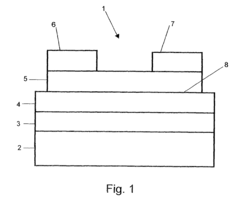
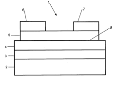
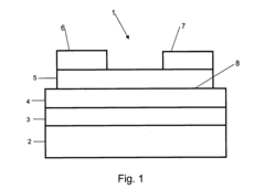
- Development of enhancement-mode, field-effect transistors with a substantially transparent channel layer made from materials like ZnO or SnO2, which are produced by annealing, and a gate insulator layer, allowing for a high optical transmission of at least 90% across the visible spectrum, enabling the creation of transparent thin-film transistors suitable for optoelectronic devices.
Transistor structures and methods for making the same
PatentInactiveUS20070141784A1
Innovation
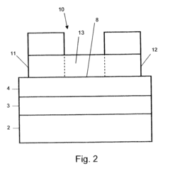
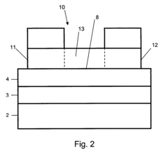
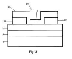
- Development of enhancement-mode, field-effect transistors with a substantially transparent channel layer made from materials like ZnO or SnO2, which are produced by annealing, and a gate insulator layer, allowing for a transparent transistor structure that enables high optical transmission across the visible and infrared spectrum.
Supply Chain Analysis for Transparent Transistor Manufacturing
The transparent transistor manufacturing supply chain represents a complex ecosystem spanning raw materials to finished devices. Silicon-based manufacturing dominates conventional transistor production, but transparent transistors require specialized materials like indium tin oxide (ITO), zinc oxide (ZnO), and indium gallium zinc oxide (IGZO). These materials face significant supply constraints, with indium being particularly critical due to its limited global reserves primarily controlled by China (approximately 70% of world production).
Material processing represents a crucial bottleneck in the supply chain. The deposition of transparent conductive oxides demands specialized equipment including physical vapor deposition (PVD) and chemical vapor deposition (CVD) systems. Leading equipment manufacturers like Applied Materials, Tokyo Electron, and ULVAC have developed proprietary solutions for these processes, creating potential dependencies for manufacturers entering this space.
Fabrication facilities present another significant challenge. While established semiconductor foundries can potentially adapt their processes for transparent transistor production, the specialized nature of these devices often requires dedicated production lines. This has led to concentration of manufacturing capabilities in East Asia, particularly Japan, South Korea, and Taiwan, where companies like Sharp, Samsung, and AUO have invested heavily in transparent electronics manufacturing infrastructure.
Testing and quality control introduce additional complexity to the supply chain. The unique optical and electrical properties of transparent transistors necessitate specialized testing equipment and protocols that differ from conventional semiconductor testing. Companies like Keysight Technologies and Advantest have begun developing dedicated solutions for this emerging market segment.
Integration capabilities represent the final critical component of the supply chain. As transparent transistors move from research to commercial applications, the ability to integrate them into end products like displays, smart windows, and transparent electronics becomes essential. This requires close collaboration between transistor manufacturers and device makers, creating potential bottlenecks in the commercialization process.
The geographical distribution of the supply chain presents both opportunities and challenges. While manufacturing is concentrated in East Asia, research and development activities are more globally distributed, with significant contributions from North America and Europe. This creates potential for regional specialization but also introduces vulnerabilities in the global supply chain that could be exacerbated by trade tensions or disruptions.
Environmental Impact and Sustainability of Transparent Electronics
The environmental footprint of transparent electronics represents a critical consideration as this technology sector expands. Transparent transistors and related components offer significant sustainability advantages compared to conventional electronics, primarily through reduced material consumption. The ultra-thin nature of transparent electronic devices requires substantially less raw material input, potentially decreasing mining activities and associated environmental degradation.
Manufacturing processes for transparent electronics are evolving toward more environmentally friendly approaches. Recent innovations in solution-based processing techniques have demonstrated up to 40% reduction in energy consumption compared to traditional semiconductor fabrication. These low-temperature manufacturing methods not only conserve energy but also minimize the emission of harmful byproducts commonly associated with conventional electronics production.
The extended lifecycle potential of transparent electronic devices presents another environmental benefit. Research indicates that oxide-based transparent transistors can maintain stable performance characteristics for significantly longer periods than silicon-based alternatives under similar operating conditions. This durability translates to reduced electronic waste generation, addressing one of the fastest-growing waste streams globally.
Recyclability represents both a challenge and opportunity within transparent electronics. While the composite nature of these devices can complicate end-of-life processing, their simplified material profiles compared to conventional electronics may ultimately facilitate more effective recycling. Industry leaders are developing specialized recovery processes for indium tin oxide and other critical materials used in transparent electronics.
Energy efficiency during operation constitutes another environmental advantage. Transparent displays utilizing advanced transistor technologies have demonstrated power consumption reductions of 15-30% compared to conventional displays of equivalent size and brightness. This efficiency gain becomes particularly significant when considering the cumulative energy savings across millions of devices over their operational lifetimes.
The integration of transparent electronics with renewable energy systems offers promising sustainability synergies. Transparent solar cells incorporating advanced transistor technologies can be seamlessly integrated into building materials, vehicle surfaces, and consumer electronics, enabling dual-functionality without additional resource consumption. This integration pathway represents one of the most promising sustainability opportunities within the transparent electronics sector.
Unlock deeper insights with Patsnap Eureka Quick Research — get a full tech report to explore trends and direct your research. Try now!
Generate Your Research Report Instantly with AI Agent
Supercharge your innovation with Patsnap Eureka AI Agent Platform!
