

What Applications Benefit from Chiplet Integration Technology
OCT 15, 20259 MIN READ
Generate Your Research Report Instantly with AI Agent
PatSnap Eureka helps you evaluate technical feasibility & market potential.
Chiplet Integration Background and Objectives
Chiplet integration technology represents a paradigm shift in semiconductor design and manufacturing, emerging as a response to the slowing of Moore's Law and the increasing challenges in traditional monolithic chip scaling. This approach involves disaggregating complex system-on-chip (SoC) designs into smaller, specialized dies called chiplets, which are then integrated using advanced packaging technologies. The evolution of chiplet technology can be traced back to the early 2010s, with significant acceleration in development over the past five years as semiconductor manufacturers sought alternatives to traditional scaling methods.
The technology has evolved from simple multi-chip modules (MCMs) to sophisticated 2.5D and 3D integration schemes, incorporating advanced interconnect technologies such as silicon interposers, organic substrates, and direct silicon-to-silicon bonding. This progression has been driven by the need to overcome physical limitations in transistor scaling while continuing to deliver performance improvements and power efficiency gains that the market demands.
The primary objectives of chiplet integration are multifaceted. First, it aims to overcome the yield challenges associated with large monolithic dies by dividing functionality across smaller chiplets, thereby improving manufacturing economics. Second, it enables the mixing of process nodes, allowing different components to be fabricated using the most appropriate technology for their specific requirements. Third, it facilitates the integration of heterogeneous technologies that may be incompatible in a single manufacturing process.
From a strategic perspective, chiplet technology also addresses the rising costs of advanced node development by extending the useful life of established process technologies. This approach allows semiconductor companies to focus their advanced node investments on components that truly benefit from cutting-edge processes, while utilizing mature nodes for other functions.
The industry trend is moving toward standardization of chiplet interfaces and protocols, as evidenced by initiatives such as the Universal Chiplet Interconnect Express (UCIe) consortium. These standardization efforts aim to create an ecosystem where chiplets from different vendors can be integrated seamlessly, potentially transforming the semiconductor industry's business model toward greater specialization and collaboration.
Looking forward, chiplet integration technology is expected to continue its trajectory of innovation, with research focusing on improving interconnect density, reducing power consumption of inter-chiplet communication, and developing more sophisticated design tools and methodologies to optimize multi-chiplet systems. The ultimate goal is to make chiplet-based design as straightforward and efficient as traditional monolithic approaches, while delivering superior performance, power efficiency, and cost-effectiveness across a wide range of applications.
Market Demand Analysis for Chiplet Solutions
The chiplet integration technology market is experiencing robust growth driven by increasing demand for advanced computing solutions across multiple sectors. Current market analysis indicates that the global chiplet market is projected to grow at a compound annual growth rate of over 40% from 2023 to 2030, reaching tens of billions of dollars by the end of the decade. This exceptional growth trajectory is primarily fueled by the escalating need for high-performance computing capabilities in data centers, artificial intelligence applications, and edge computing environments.
Data center operators represent one of the largest market segments for chiplet technology, as they continuously seek more efficient and powerful processing solutions to handle exponentially growing workloads. The demand is particularly strong in hyperscale data centers where power efficiency, computational density, and total cost of ownership are critical factors driving technology adoption decisions.
The artificial intelligence and machine learning sector presents another significant market opportunity for chiplet solutions. As AI models grow increasingly complex, traditional monolithic chip designs struggle to deliver the necessary computational power within acceptable power envelopes. Market research indicates that AI accelerator chips utilizing chiplet architecture could capture over 30% of the AI chip market within the next five years, representing a substantial growth opportunity.
High-performance computing (HPC) applications in scientific research, weather forecasting, and complex simulations constitute another key market segment. These applications require massive parallel processing capabilities that chiplet-based designs can efficiently deliver through specialized processing elements working in concert.
Consumer electronics manufacturers are also showing increasing interest in chiplet technology, particularly for premium smartphones, tablets, and gaming devices. The ability to integrate heterogeneous components optimized for specific functions (CPU, GPU, AI, connectivity) while maintaining power efficiency is highly attractive for next-generation mobile devices.
Automotive applications represent an emerging but rapidly growing market for chiplet solutions, driven by the increasing computational requirements of advanced driver assistance systems (ADAS) and autonomous driving platforms. The automotive sector values the reliability, performance, and potential for functional safety certification that modular chiplet designs can offer.
Market analysis reveals that geographic distribution of demand is concentrated in North America and Asia-Pacific regions, with major technology companies and semiconductor manufacturers leading adoption. However, European markets are showing accelerated growth rates as regional initiatives promote technological sovereignty in semiconductor design and manufacturing.
Current Chiplet Technology Landscape and Challenges
Chiplet integration technology has evolved significantly over the past decade, transforming from an experimental approach to a mainstream semiconductor manufacturing strategy. The current landscape shows widespread adoption across major semiconductor companies including AMD, Intel, TSMC, and Samsung, each developing proprietary chiplet architectures and integration methodologies. This fragmentation presents significant challenges for standardization and interoperability between different vendors' chiplet solutions.
The primary technical challenges facing chiplet integration today center around interconnect technologies. While advanced packaging solutions like EMIB (Embedded Multi-die Interconnect Bridge) from Intel and CoWoS (Chip-on-Wafer-on-Substrate) from TSMC have demonstrated impressive bandwidth capabilities, they still face limitations in terms of power efficiency, signal integrity, and thermal management when scaling to more complex multi-chiplet designs.
Die-to-die interfaces represent another critical challenge area. Current standards like UCIe (Universal Chiplet Interconnect Express) are gaining traction but have yet to achieve universal adoption. The industry continues to struggle with balancing proprietary performance advantages against the benefits of standardized interfaces that would enable a more robust chiplet ecosystem and marketplace.
Testing methodologies for multi-chiplet systems present unique difficulties not encountered in monolithic designs. Known-good-die testing becomes increasingly complex when considering the interactions between multiple chiplets, and yield management strategies must evolve to account for the compound effects of integrating multiple silicon components.
From a manufacturing perspective, the supply chain for chiplet-based products introduces new complexities. Different chiplets may be manufactured using different process nodes, potentially at different foundries, requiring sophisticated coordination and quality control systems. This distributed manufacturing approach creates both opportunities for optimization and challenges for consistent production.
Thermal management represents a persistent challenge, particularly in high-performance computing applications. The concentration of processing elements and the interfaces between chiplets create thermal hotspots that require innovative cooling solutions. Current approaches include advanced thermal interface materials and integrated liquid cooling channels, though optimal solutions remain application-specific.
Geographically, chiplet technology development shows concentration in East Asia (particularly Taiwan and South Korea), the United States, and to a lesser extent Europe. This distribution reflects the broader semiconductor manufacturing landscape but introduces potential supply chain vulnerabilities that industry and governments are increasingly seeking to address through initiatives like the CHIPS Act in the United States and similar programs in Europe.
Current Chiplet Integration Methodologies
01 Advanced Packaging Technologies for Chiplet Integration
Advanced packaging technologies are essential for chiplet integration, enabling multiple dies to be combined into a single package. These technologies include 2.5D and 3D integration methods, interposer-based solutions, and fan-out wafer-level packaging. These approaches allow for higher performance, reduced power consumption, and improved thermal management in multi-die systems while maintaining high-bandwidth connections between chiplets.- Advanced Packaging Technologies for Chiplet Integration: Advanced packaging technologies are crucial for chiplet integration, enabling multiple dies to be combined into a single package. These technologies include 2.5D and 3D integration methods, interposer-based solutions, and fan-out wafer-level packaging. These approaches allow for heterogeneous integration of chiplets with different functionalities, process nodes, or from different manufacturers, while maintaining high performance interconnections between the dies.
- Interconnect Technologies for Chiplet Communication: Interconnect technologies are essential for enabling efficient communication between chiplets. These include high-bandwidth, low-latency interfaces such as silicon bridges, through-silicon vias (TSVs), and advanced micro-bumps. Novel interconnect architectures optimize data transfer between chiplets while minimizing power consumption and signal degradation, which is critical for maintaining system performance in multi-chiplet designs.
- Thermal Management Solutions for Chiplet Designs: Thermal management is a significant challenge in chiplet integration due to the high power density and heat generation in compact multi-die packages. Solutions include advanced thermal interface materials, integrated heat spreaders, microchannel cooling systems, and thermal-aware placement of chiplets. Effective thermal management ensures reliable operation and prevents performance degradation due to thermal throttling in chiplet-based systems.
- Design and Testing Methodologies for Chiplet-Based Systems: Specialized design and testing methodologies are required for chiplet-based systems to ensure functionality and reliability. These include design-for-test approaches, known-good-die testing before integration, built-in self-test capabilities, and standardized interfaces. Advanced simulation tools and design automation software help manage the complexity of chiplet integration, enabling efficient verification and validation of multi-die systems.
- Standardization and Ecosystem Development for Chiplet Integration: Standardization efforts are crucial for the widespread adoption of chiplet technology. Industry consortia are developing open standards for chiplet interfaces, protocols, and physical design specifications. These standards enable interoperability between chiplets from different vendors, fostering a robust ecosystem where designers can mix and match chiplets from various sources to create customized solutions. Standardization reduces development costs and accelerates time-to-market for chiplet-based products.
02 Interconnect Technologies for Chiplet-to-Chiplet Communication
Interconnect technologies are crucial for enabling efficient communication between chiplets. These include advanced die-to-die interfaces, through-silicon vias (TSVs), micro-bumps, and high-density redistribution layers. These interconnect solutions provide high bandwidth, low latency, and power-efficient communication channels between chiplets, which is essential for maintaining system performance in disaggregated chip designs.Expand Specific Solutions03 Thermal Management Solutions for Chiplet Designs
Thermal management is a critical aspect of chiplet integration technology. Various solutions have been developed to address heat dissipation challenges in multi-die packages, including integrated heat spreaders, thermal interface materials, and advanced cooling techniques. These solutions help maintain optimal operating temperatures across different chiplets with varying thermal profiles, ensuring reliable performance and longevity of the integrated system.Expand Specific Solutions04 Design and Testing Methodologies for Chiplet-Based Systems
Specialized design and testing methodologies have been developed for chiplet-based systems. These include design automation tools for multi-die integration, known-good-die testing approaches, and post-assembly validation techniques. These methodologies address the unique challenges of designing and verifying heterogeneous integrated systems, ensuring functional correctness, signal integrity, and reliability across chiplet boundaries.Expand Specific Solutions05 Standardization and Interoperability Frameworks for Chiplets
Standardization efforts are emerging to enable interoperability between chiplets from different vendors. These include interface protocols, physical design specifications, and power delivery standards. Such frameworks aim to create an ecosystem where chiplets can be mixed and matched like building blocks, allowing for more flexible system design, reduced development costs, and accelerated time-to-market for complex semiconductor products.Expand Specific Solutions
Key Industry Players in Chiplet Ecosystem
Chiplet integration technology is currently in a growth phase, with the market expanding rapidly due to increasing demand for high-performance computing solutions. The global chiplet market is projected to reach significant scale as major players advance their integration strategies. Companies like TSMC, Intel, and AMD are leading the technological development, with TSMC's advanced packaging technologies and Intel's EMIB and Foveros architectures demonstrating high maturity levels. AMD has successfully commercialized chiplet designs in their processors, while Huawei and SMIC are making strategic investments to close the gap. Applications benefiting most include high-performance computing, AI accelerators, data centers, and edge computing devices, where the technology enables better performance scaling, power efficiency, and cost optimization compared to monolithic designs.
Taiwan Semiconductor Manufacturing Co., Ltd.
Technical Solution: TSMC's chiplet integration technology centers around their advanced packaging solutions, including Chip-on-Wafer-on-Substrate (CoWoS) and System-on-Integrated-Chips (SoIC). These technologies enable the integration of multiple silicon dies in a single package with high-bandwidth, low-latency interconnects. TSMC's 3DFabric platform combines front-end and back-end technologies to create a comprehensive 3D silicon stacking and advanced packaging solution. This approach allows system designers to disaggregate traditional monolithic SoCs into smaller chiplets that can be manufactured using optimal process nodes for each function. TSMC's technology has been particularly impactful for high-performance computing applications, enabling products like AMD's EPYC processors and various AI accelerators that require massive parallel computing capabilities and memory bandwidth. The company's InFO (Integrated Fan-Out) packaging technology has also been crucial for mobile applications, allowing for thinner packages with improved thermal performance.
Strengths: Industry-leading interconnect density and bandwidth; mature manufacturing processes ensuring high yields; extensive ecosystem support for design and implementation. Weaknesses: Higher initial costs compared to traditional packaging; requires sophisticated design tools and expertise; thermal management challenges in densely packed chiplet configurations.
Intel Corp.
Technical Solution: Intel's chiplet integration technology, branded as "Foveros," represents a 3D packaging approach that vertically stacks compute tiles. This technology enables the integration of heterogeneous chiplets manufactured using different process nodes, allowing Intel to combine high-performance cores with power-efficient cores and specialized accelerators in a single package. Intel's Meteor Lake processors utilize this technology to integrate CPU, GPU, NPU, and I/O components as separate tiles. The company has further advanced this with Foveros Omni and Foveros Direct, which offer enhanced interconnect density and reduced power consumption. Applications benefiting from Intel's chiplet approach include high-performance computing systems, AI accelerators, and power-efficient mobile computing platforms where different functional blocks can be optimized separately and then integrated into a unified system.
Strengths: Allows mixing of process nodes for cost optimization; enables heterogeneous integration of specialized components; reduces time-to-market by reusing validated chiplet designs. Weaknesses: Thermal management challenges in 3D stacked configurations; higher manufacturing complexity; potential yield issues when integrating multiple chiplets.
Core Chiplet Interconnect Technologies Analysis
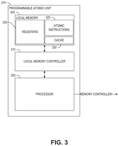
Detecting infinite loops in a programmable atomic transaction
PatentActiveUS20240311149A1
Innovation
- Implementing a method within the programmable atomic unit to detect and terminate programmable atomic transactions that exceed a predetermined instruction execution limit, using an instruction counter to monitor execution and send a response to the calling processor if the limit is reached, thereby freeing resources and preventing system stalls.
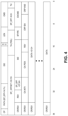
Assembly having a face-to-face bonded chiplet
PatentWO2025042587A1
Innovation
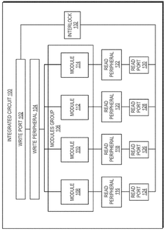
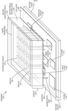
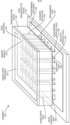
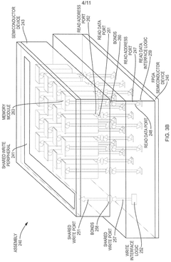
- The proposed integrated circuit architecture features a face-to-face bonded chiplet configuration, incorporating a shared write port and multiple read ports, along with a network-on-chip fabric, to enable efficient communication and data management across multiple semiconductor devices.
Thermal Management Considerations in Chiplet Designs
Thermal management represents a critical challenge in chiplet integration technology, as the disaggregation of system components into multiple dies introduces complex heat dissipation dynamics. The increased transistor density within chiplet designs creates concentrated heat zones that require sophisticated cooling solutions. When multiple chiplets are integrated within a single package, thermal coupling between adjacent dies can lead to performance bottlenecks and reliability concerns if not properly addressed.
The thermal interface materials (TIMs) between chiplets and heat spreaders play a crucial role in efficient heat transfer. Advanced TIMs with higher thermal conductivity are being developed specifically for chiplet architectures to minimize thermal resistance at these critical junctions. Additionally, the interposer or substrate material selection significantly impacts overall thermal performance, with materials like silicon and aluminum nitride offering superior thermal conductivity compared to traditional organic substrates.
Power delivery networks in chiplet designs must be carefully engineered to distribute power efficiently while minimizing thermal hotspots. The non-uniform power distribution across different functional chiplets necessitates targeted cooling strategies that address the unique thermal profile of each component. High-performance computing applications utilizing chiplet technology often implement liquid cooling solutions to manage the extreme thermal loads generated during intensive computational tasks.
Thermal simulation and modeling have become essential tools in chiplet design workflows. Multi-physics simulations that account for electrical, mechanical, and thermal interactions enable designers to predict hotspots and optimize thermal management strategies before physical prototyping. These simulation approaches must consider both steady-state and transient thermal behaviors to ensure reliable operation under varying workloads.
Dynamic thermal management techniques, including adaptive frequency scaling and workload migration between chiplets, offer runtime solutions to thermal challenges. These approaches leverage temperature sensors embedded within the chiplet package to monitor thermal conditions and adjust system behavior accordingly. The integration of these sensors must be carefully planned to provide accurate temperature data without introducing additional thermal or electrical complications.
As chiplet integration advances toward three-dimensional stacking configurations, thermal management becomes exponentially more challenging. Heat generated by chiplets in lower layers must traverse through multiple dies and bonding layers before reaching the primary heat dissipation mechanism. Novel cooling approaches, including through-silicon vias (TSVs) dedicated to thermal conduction and microfluidic cooling channels integrated within the chiplet stack, are being explored to address these emerging thermal challenges.
Standardization Efforts in Chiplet Interfaces
The standardization of chiplet interfaces represents a critical foundation for the widespread adoption and evolution of chiplet integration technology. Industry consortia like the Universal Chiplet Interconnect Express (UCIe) have emerged as pivotal forces in establishing common protocols and specifications for chiplet-to-chiplet communication. UCIe, backed by industry giants including Intel, AMD, Arm, and TSMC, aims to create an open ecosystem where chiplets from different vendors can seamlessly interoperate.
Beyond UCIe, other significant standardization initiatives include the Open Compute Project's Bunch of Wires (BoW) specification, which focuses on providing a simpler, cost-effective alternative for chiplet interconnects. The Advanced Interface Bus (AIB) from Intel and the High Bandwidth Memory (HBM) interface standard also contribute to the standardization landscape, each addressing specific aspects of chiplet integration requirements.
These standardization efforts are addressing several key technical challenges. Power efficiency in inter-chiplet communication remains paramount, with standards increasingly focusing on reducing the energy cost per bit transferred. Physical interconnect density represents another critical area, as standards must enable more connections in smaller spaces to support the miniaturization trend in chiplet design.
Signal integrity across chiplet boundaries constitutes a significant standardization focus, particularly as data rates continue to increase. Standards must define protocols that maintain reliable communication while managing crosstalk and electromagnetic interference between closely packed chiplets. Additionally, thermal management considerations are being incorporated into interface standards to address the concentrated heat generation in multi-chiplet packages.
The economic implications of standardization cannot be overstated. By establishing common interfaces, the industry is moving toward a more modular semiconductor ecosystem where specialized chiplets can be designed once and reused across multiple products. This approach potentially reduces development costs and time-to-market while enabling more customized solutions through the mixing and matching of standardized components.
Looking forward, emerging standards are beginning to address heterogeneous integration challenges, where chiplets manufactured using different process technologies must work together seamlessly. The evolution of these standards will significantly influence which applications can most effectively leverage chiplet integration technology, potentially expanding benefits beyond high-performance computing to more cost-sensitive market segments.
Unlock deeper insights with PatSnap Eureka Quick Research — get a full tech report to explore trends and direct your research. Try now!
Generate Your Research Report Instantly with AI Agent
Supercharge your innovation with PatSnap Eureka AI Agent Platform!