What Does OLED vs MicroLED Mean for Future Technologies
OCT 24, 20259 MIN READ
Generate Your Research Report Instantly with AI Agent
Patsnap Eureka helps you evaluate technical feasibility & market potential.
OLED vs MicroLED: Evolution and Objectives
Display technologies have undergone significant evolution since the introduction of cathode ray tubes (CRTs) in the early 20th century. The transition from CRTs to liquid crystal displays (LCDs) marked the first major shift toward flatter, more energy-efficient screens. OLED (Organic Light-Emitting Diode) technology emerged in the late 1980s, with the first commercial applications appearing in the early 2000s, revolutionizing display technology with its self-emissive properties, eliminating the need for backlighting.
MicroLED represents the latest advancement in this evolutionary chain, first demonstrated in laboratories in the early 2000s but only recently approaching commercial viability. Unlike OLEDs that use organic compounds, MicroLEDs utilize inorganic gallium nitride-based materials, offering potentially superior performance characteristics while maintaining the self-emissive advantages pioneered by OLED technology.
The technological trajectory clearly indicates a movement toward displays that offer higher efficiency, better color reproduction, faster response times, and increased durability. Both OLED and MicroLED technologies align with this trend, though they represent different approaches to achieving these objectives. The industry's primary goals include developing displays with perfect black levels, infinite contrast ratios, wider color gamuts, and reduced power consumption.
Current technical objectives for both technologies include overcoming manufacturing challenges to reduce production costs, improving longevity (particularly addressing the burn-in issues that plague OLED), and scaling production capabilities to meet growing market demands. For OLED specifically, research focuses on extending the lifespan of blue organic materials, which traditionally degrade faster than red and green components.
MicroLED development aims to perfect mass transfer techniques for placing millions of microscopic LEDs precisely onto substrates—a significant manufacturing hurdle. Additionally, researchers are working to improve the efficiency of green and red MicroLEDs to match their blue counterparts, as well as reducing the minimum achievable pixel size to enable higher resolution displays in smaller form factors.
Both technologies are being developed with flexibility and transparency capabilities in mind, opening new application possibilities beyond traditional displays. The ultimate objective is to create display technologies that can seamlessly integrate into various environments and use cases, from smartphones and televisions to automotive displays, augmented reality glasses, and even architectural elements.
The competition between OLED and MicroLED is driving rapid innovation, with each technology pushing the boundaries of what's possible in display performance. This technological rivalry benefits consumers and industries alike, accelerating the development timeline for next-generation display solutions that will fundamentally transform how we interact with visual information.
Market Demand Analysis for Advanced Display Technologies
The global display technology market is witnessing a significant shift towards advanced solutions, with OLED (Organic Light Emitting Diode) and MicroLED technologies at the forefront of this transformation. Current market analysis indicates that the advanced display market is expected to reach $167 billion by 2025, growing at a CAGR of approximately 18.5% from 2020.
Consumer electronics remains the primary driver for advanced display technologies, with smartphones accounting for nearly 40% of the OLED market share. The demand for thinner, lighter, and more energy-efficient displays with superior color reproduction capabilities continues to fuel the adoption of OLED technology across various product categories including televisions, wearables, and automotive displays.
MicroLED, though still in its early commercialization phase, is generating substantial interest from premium market segments. The technology's promise of higher brightness, longer lifespan, and better energy efficiency compared to OLED has created a growing demand in specialized applications such as AR/VR headsets, smartwatches, and high-end televisions. Market research indicates that the MicroLED segment is expected to grow at over 80% annually for the next five years, albeit from a smaller base.
Regional analysis reveals that Asia-Pacific dominates the manufacturing landscape for both technologies, with South Korea and China leading OLED production while Taiwan and Japan focus increasingly on MicroLED development. North America and Europe represent significant consumer markets, with particular emphasis on premium applications where visual performance is paramount.
Industry surveys indicate that consumers are increasingly willing to pay premium prices for superior display quality, with 67% of high-end smartphone buyers citing display quality as a critical purchase factor. This trend extends to the television market, where the premium segment (>$1,500) has grown by 24% annually despite overall market saturation.
The automotive sector represents an emerging opportunity for both technologies, with projections suggesting that advanced displays will be incorporated into 60% of new vehicles by 2025. The demand is driven by both aesthetic considerations and functional requirements for heads-up displays and infotainment systems that perform well under varying lighting conditions.
Commercial applications including digital signage, retail displays, and control room monitors are also showing increased adoption rates, with businesses valuing the visual impact, space savings, and potential energy efficiency benefits of next-generation display technologies. This segment is projected to grow at 22% annually through 2025.
The healthcare and aerospace/defense sectors represent smaller but high-value market segments, where the superior visual performance and reliability of MicroLED technology in particular is expected to command significant price premiums and drive innovation in specialized applications.
Current Technical Limitations and Challenges
Despite significant advancements in both OLED and MicroLED technologies, several technical limitations and challenges persist that impede their widespread adoption across various applications. OLED technology, while commercially established, continues to face durability issues with organic materials degrading over time, particularly blue OLEDs which have shorter lifespans than red and green counterparts. This differential aging leads to color shifts and reduced display quality over extended usage periods. Additionally, OLED panels remain susceptible to burn-in effects when static images are displayed for prolonged periods, limiting their application in scenarios requiring constant information display.
Manufacturing scalability presents another significant challenge for OLED technology. While small and medium-sized OLED panels have achieved production efficiency, large-format displays still face yield issues and high production costs. The vacuum deposition processes required for OLED manufacturing are complex and resource-intensive, contributing to higher end-product pricing compared to conventional display technologies.
MicroLED technology, though promising, faces even more substantial manufacturing hurdles. The mass transfer process—moving millions of microscopic LED chips from growth substrates to display backplanes with precise positioning—remains the most significant technical bottleneck. Current yield rates for this process are suboptimal, dramatically increasing production costs. The industry has yet to develop a universally effective mass transfer technique that balances speed, accuracy, and cost-effectiveness at commercial scale.
Color consistency across MicroLED displays presents another technical challenge. Due to the nature of LED chip production, achieving uniform brightness and color reproduction across millions of individual emitters requires sophisticated compensation algorithms and manufacturing precision beyond current industry standards. The smaller the MicroLED chips become, the more pronounced these uniformity issues become.
Power efficiency, while theoretically superior in MicroLED technology, faces practical implementation challenges. The driving circuits for MicroLED displays must manage millions of individual pixels with precise current control, requiring complex backplane designs that can offset some of the technology's inherent efficiency advantages, particularly in high-resolution applications.
Both technologies also face materials science challenges. OLED requires continued development of more stable organic compounds and better encapsulation methods to prevent moisture and oxygen degradation. MicroLED needs advancements in epitaxial growth techniques to improve efficiency and reduce defect rates in ultra-small LED structures, particularly for blue and green emitters which lag behind red in efficiency metrics.
Addressing these technical limitations requires coordinated efforts across multiple disciplines, including materials science, manufacturing engineering, and electronic design. The resolution of these challenges will largely determine which technology ultimately dominates in specific application segments of the future display market.
Current Implementation Solutions and Approaches
01 OLED display performance characteristics
OLED displays offer superior performance characteristics including high contrast ratios, wide color gamut, and fast response times. These self-emissive displays eliminate the need for backlighting, allowing for true blacks and excellent viewing angles. OLED technology enables flexible and transparent display applications while consuming less power when displaying darker content compared to traditional LCD displays.- OLED display technology performance characteristics: OLED (Organic Light Emitting Diode) displays offer superior performance characteristics including high contrast ratios, wide viewing angles, and fast response times. These self-emissive displays eliminate the need for backlighting, allowing for thinner device profiles and lower power consumption when displaying dark content. OLED technology enables flexible and foldable display applications due to its thin-film structure and provides excellent color reproduction with deep blacks and vibrant colors.
- MicroLED display technology advantages: MicroLED displays utilize arrays of microscopic LED elements that are self-emissive, offering several performance advantages including higher brightness, improved energy efficiency, and longer lifespan compared to other display technologies. These displays provide exceptional pixel density, superior color gamut, and faster refresh rates while maintaining high contrast ratios. MicroLED technology also demonstrates better resistance to burn-in issues and can be manufactured in various form factors for different applications.
- Display driver and control systems for enhanced performance: Advanced driver and control systems are crucial for optimizing the performance of both OLED and MicroLED displays. These systems manage pixel addressing, current control, and timing synchronization to ensure uniform brightness and color accuracy across the display. Sophisticated compensation algorithms correct for variations in electrical characteristics of individual pixels, while pulse width modulation techniques enable precise grayscale control and high dynamic range. These control systems also implement power management strategies to balance visual performance with energy efficiency.
- Pixel structure and materials innovation: Innovations in pixel structure and materials significantly impact display performance in both OLED and MicroLED technologies. Advanced pixel architectures incorporate specialized subpixel arrangements and light extraction features to improve efficiency and color accuracy. Novel semiconductor materials and emitter compounds enhance quantum efficiency and spectral purity, while specialized encapsulation techniques protect sensitive components from environmental degradation. These material innovations contribute to improved brightness, color gamut, and operational stability of the displays.
- Integration technologies for display systems: Integration technologies focus on combining display panels with supporting components to create complete display systems with optimized performance. These include advanced bonding techniques for attaching driver ICs and flexible circuits, thermal management solutions to dissipate heat and maintain consistent operation, and optical enhancement films to improve viewing characteristics. Integration approaches also address challenges in scaling manufacturing processes while maintaining quality, and enable features such as in-display sensors, cameras, and touch functionality without compromising display performance.
02 MicroLED display technology advantages
MicroLED displays provide exceptional brightness, energy efficiency, and longevity compared to other display technologies. These displays utilize arrays of microscopic LED elements that are self-emissive, offering improved luminance efficiency and color purity. MicroLED technology enables higher pixel density, better durability, and resistance to burn-in issues that can affect OLED displays, making them suitable for high-performance applications.Expand Specific Solutions03 Display driver and control systems
Advanced driver and control systems are crucial for optimizing the performance of both OLED and MicroLED displays. These systems manage pixel addressing, current control, and timing synchronization to ensure uniform brightness and color accuracy across the display. Innovations in driving circuits help reduce power consumption while maintaining display quality and extending the operational lifespan of these advanced display technologies.Expand Specific Solutions04 Pixel structure and light emission efficiency
The pixel structure in OLED and MicroLED displays significantly impacts overall display performance. Innovations in pixel design focus on improving light emission efficiency, reducing current leakage, and enhancing color purity. Advanced pixel architectures incorporate specialized materials and structures to optimize quantum efficiency and light extraction, resulting in displays with higher brightness, better color accuracy, and improved energy efficiency.Expand Specific Solutions05 Integration technologies for flexible and foldable displays
Integration technologies enable the development of flexible, foldable, and curved OLED and MicroLED displays. These technologies involve specialized substrate materials, encapsulation methods, and interconnect solutions that maintain display performance while allowing physical deformation. Advanced integration approaches address challenges related to mechanical stress, thermal management, and uniform light emission across bendable surfaces, expanding the application possibilities for next-generation display products.Expand Specific Solutions
Key Industry Players and Competitive Landscape
The OLED vs MicroLED technology landscape is currently in a transitional phase, with OLED being more mature and commercially established while MicroLED represents an emerging disruptive technology. The global display market is projected to reach $200 billion by 2025, with these advanced technologies capturing increasing market share. In terms of technical maturity, companies like Samsung, BOE Technology, and LG Display lead OLED commercialization with established manufacturing capabilities. For MicroLED, companies including Samsung, Apple, and BOE are investing heavily in R&D but face significant manufacturing challenges. Smaller specialized firms like OLEDWorks and Lumileds are developing niche applications, while Chinese manufacturers such as BOE and TCL's China Star Optoelectronics are rapidly advancing their technical capabilities to challenge traditional market leaders.
BOE Technology Group Co., Ltd.
Technical Solution: BOE has established itself as a major player in display technologies, with significant investments in both OLED and MicroLED. For OLED, BOE employs flexible AMOLED technology using low-temperature polysilicon (LTPS) backplanes, enabling thin, bendable displays with high color saturation. They've developed specialized vapor deposition techniques for organic material application and have achieved mass production capabilities for smartphone and tablet displays. In the MicroLED space, BOE has created prototype displays using chip-scale packaging technology with LED chips under 50 micrometers. Their MicroLED approach incorporates a unique mass transfer process that utilizes electrostatic forces to precisely position microLED chips onto TFT substrates. BOE has demonstrated MicroLED displays with pixel densities exceeding 1,000 PPI and has established partnerships with multiple device manufacturers to accelerate commercialization. Their R&D efforts focus on improving transfer yield rates and reducing production costs through automated manufacturing processes.
Strengths: Extensive manufacturing infrastructure; strong position in the Chinese display market; vertical integration capabilities; significant R&D investment in transfer technologies for MicroLED. Weaknesses: Still catching up to Samsung and LG in premium OLED market segments; MicroLED technology remains primarily in prototype phase with limited commercial products; challenges in achieving cost-effective mass production for consumer applications.
Wuhan China Star Optoelectronics Technology Co., Ltd.
Technical Solution: Wuhan China Star Optoelectronics Technology (CSOT) has developed comprehensive solutions in both OLED and MicroLED technologies. For OLED, CSOT employs advanced vapor deposition techniques with multi-stack organic layers to enhance luminous efficiency and display lifespan. Their OLED panels feature oxide TFT backplanes that deliver improved electron mobility and stability compared to conventional a-Si TFTs. CSOT has achieved mass production of flexible OLED panels with integrated touch functionality through their proprietary "touch-in-cell" technology. In the MicroLED domain, CSOT has developed a unique "micro-transfer printing" process that enables simultaneous transfer of multiple LED chips with positioning accuracy below 1 micrometer. Their MicroLED displays incorporate specialized phosphor conversion layers that enhance color gamut while reducing the complexity of RGB chip manufacturing. CSOT has demonstrated MicroLED prototypes with pixel densities of 1,200 PPI and contrast ratios exceeding 1,000,000:1, positioning their technology for next-generation AR/VR applications.
Strengths: Strong manufacturing capabilities as part of TCL Group; innovative transfer printing technology for MicroLED; established production lines for OLED with growing capacity. Weaknesses: Less international brand recognition compared to competitors; still developing high-volume manufacturing processes for MicroLED; challenges in achieving cost parity with established display technologies.
Core Patents and Technical Innovations
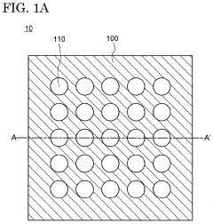
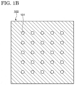
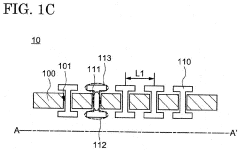
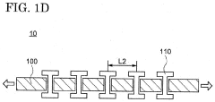
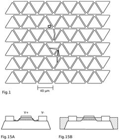
Element transfer device and element transfer method
PatentPendingUS20220262665A1
Innovation
- An element transfer device with an elastic sheet and pickup portions, including a shaft portion and head portions, that can adjust its distance between pickup points to match the spacing on both the element and circuit substrates, allowing for simultaneous transfer of multiple micro LEDs.
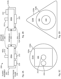
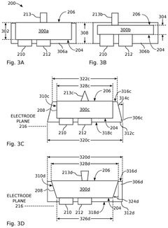
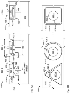
Encapsulated light emitting diodes for selective fluidic assembly
PatentActiveUS12119432B2
Innovation
- The use of partially encapsulated semiconductor-based inorganic micro-LEDs with a patternable polymer encapsulant that protects the LEDs from collisions and optimizes their shape for efficient assembly, allowing for higher speed and yield while preventing defects, and enabling precise alignment of LED colors on a display substrate.
Environmental Impact and Sustainability Considerations
The environmental impact of display technologies has become increasingly important as consumer electronics proliferate globally. OLED and MicroLED technologies present distinct environmental profiles throughout their lifecycles, from manufacturing to disposal. Understanding these differences is crucial for sustainable technology development.
OLED manufacturing processes generally require fewer materials and less energy compared to traditional LCD displays. However, they still utilize rare earth elements and organic compounds that pose extraction and disposal challenges. The production process involves potentially harmful chemicals, including heavy metals like cadmium in some formulations, though manufacturers have made significant progress in developing cadmium-free alternatives.
MicroLED manufacturing, while still evolving, presents its own environmental considerations. The production process is currently more energy-intensive than OLED manufacturing, primarily due to the complex transfer process of placing millions of microscopic LEDs precisely onto substrates. However, MicroLED displays contain fewer toxic substances overall and do not require the organic compounds that can be problematic in OLED disposal.
Power consumption represents a critical environmental factor for display technologies. OLEDs offer pixel-level control that enables significant energy savings, particularly when displaying darker content. MicroLED technology promises even greater energy efficiency at scale, with potential power consumption reductions of 30-50% compared to OLEDs when operating at full brightness, translating to extended device battery life and reduced charging frequency.
Longevity and durability significantly impact environmental sustainability. OLED displays typically suffer from organic material degradation over time, leading to shorter lifespans (approximately 30,000-60,000 hours) and more frequent replacement cycles. MicroLED technology offers substantially longer theoretical lifespans exceeding 100,000 hours, potentially reducing electronic waste through less frequent device replacement.
End-of-life considerations reveal further distinctions. OLED panels present recycling challenges due to their organic materials and thin-film construction. MicroLED displays, composed primarily of inorganic materials, may offer more straightforward recycling pathways, though the miniaturization of components presents its own recovery challenges.
Carbon footprint assessments across the complete lifecycle indicate that while MicroLED manufacturing currently generates higher emissions, the extended lifespan and superior energy efficiency may result in a lower overall environmental impact. As manufacturing processes mature and scale, this advantage is expected to increase further, positioning MicroLED as potentially the more sustainable long-term display solution.
Supply Chain Analysis and Manufacturing Scalability
The supply chain for OLED and MicroLED technologies represents a critical factor in their respective market adoption trajectories. OLED manufacturing has matured significantly over the past decade, with established supply chains primarily dominated by South Korean companies like Samsung and LG Display, alongside emerging Chinese manufacturers. The production process has been refined to achieve economies of scale, particularly for small and medium-sized displays, though yield rates for larger panels remain challenging.
In contrast, MicroLED supply chains are still in nascent stages of development, characterized by fragmentation and technological bottlenecks. The manufacturing process requires unprecedented precision in transferring millions of microscopic LED chips to substrates with near-perfect yield rates. Current mass transfer techniques struggle to achieve the necessary efficiency for cost-effective production at scale, creating a significant barrier to commercialization.
Raw material considerations also differentiate these technologies. OLED production relies heavily on organic compounds and rare metals like indium, which face potential supply constraints as demand increases. MicroLED manufacturing depends on semiconductor materials like gallium nitride, which benefits from established semiconductor industry supply chains but requires adaptation for the unique demands of display production.
Equipment suppliers represent another crucial element in the ecosystem. OLED manufacturing equipment has become increasingly specialized, with companies like Applied Materials and Canon Tokki developing proprietary solutions. The MicroLED equipment market remains underdeveloped, with significant R&D investment required to create tools capable of high-precision, high-volume production.
Scalability challenges differ markedly between technologies. OLED manufacturing has achieved reasonable scalability for smartphone displays but faces persistent yield challenges for larger formats. MicroLED confronts more fundamental scalability hurdles, particularly in the mass transfer process and defect management, which currently prevent cost-effective mass production.
Regional manufacturing capabilities also influence future technology adoption. East Asian countries maintain dominance in OLED production, while MicroLED development occurs across a more globally distributed research network, potentially enabling new manufacturing centers to emerge as the technology matures.
The supply chain resilience of both technologies will ultimately determine their market penetration. OLED's more mature but concentrated supply chain presents different risks compared to MicroLED's emerging but fragmented ecosystem. Companies investing in either technology must carefully evaluate these supply chain dynamics when formulating long-term product strategies.
Unlock deeper insights with Patsnap Eureka Quick Research — get a full tech report to explore trends and direct your research. Try now!
Generate Your Research Report Instantly with AI Agent
Supercharge your innovation with Patsnap Eureka AI Agent Platform!