Why OLED vs MicroLED are Pivotal in Display Engineering
OCT 24, 20259 MIN READ
Generate Your Research Report Instantly with AI Agent
Patsnap Eureka helps you evaluate technical feasibility & market potential.
OLED and MicroLED Display Evolution and Objectives
Display technology has undergone remarkable evolution since the introduction of cathode ray tubes in the early 20th century. The journey from CRTs to LCDs represented the first major paradigm shift, but today we stand at another pivotal transition point between OLED (Organic Light Emitting Diode) and MicroLED technologies. These advanced display technologies are not merely incremental improvements but fundamental reimaginings of how visual information is presented.
OLED technology emerged commercially in the late 1990s, pioneered by companies like Kodak and Sony. The technology's fundamental innovation lies in its self-emissive nature, eliminating the need for backlighting required in LCD displays. This breakthrough enabled thinner, more flexible displays with superior contrast ratios and energy efficiency. The evolution of OLED has progressed through several generations, from passive-matrix to active-matrix designs, and more recently to flexible and transparent implementations.
MicroLED represents the next frontier in display engineering, with roots dating back to the early 2000s but gaining significant momentum only in the past decade. Unlike OLEDs that use organic compounds, MicroLEDs utilize inorganic gallium nitride-based materials at microscopic scales. This fundamental material difference addresses several limitations of OLED technology, particularly regarding longevity and brightness capabilities.
The technical objectives driving both technologies reflect the industry's pursuit of the "perfect display" – one that combines infinite contrast, perfect color reproduction, maximum energy efficiency, durability, and form factor flexibility. OLED has already achieved commercial success in premium smartphones, televisions, and wearables, while MicroLED is positioned as the technology that may eventually supersede it, particularly in high-end applications where performance justifies cost premiums.
Current technical objectives for OLED development include addressing burn-in issues, improving blue pixel longevity, enhancing brightness for HDR applications, and reducing production costs. For MicroLED, the primary objectives revolve around overcoming mass production challenges, improving transfer yields of microscopic LED elements, reducing power consumption, and achieving cost structures that enable broader market adoption.
The convergence of these display technologies with other emerging fields such as augmented reality, virtual reality, and ambient computing is creating new technical imperatives. Both technologies must evolve to support higher pixel densities, faster refresh rates, and more sophisticated integration with sensing technologies while maintaining energy efficiency – particularly critical for battery-powered devices.
Understanding the evolutionary paths and technical objectives of these display technologies is essential for predicting future market dynamics and identifying strategic investment opportunities in the display engineering ecosystem.
Market Demand Analysis for Advanced Display Technologies
The display technology market is witnessing unprecedented growth driven by consumer electronics, automotive interfaces, and commercial signage applications. Current market analysis indicates that the global advanced display market is projected to reach $167 billion by 2025, with OLED technology currently holding approximately 20% market share while MicroLED is emerging rapidly with significant year-over-year growth rates exceeding 80% in specialized applications.
Consumer demand for superior visual experiences continues to fuel innovation in display technologies. Smartphones remain the primary driver for OLED adoption, with premium handsets from major manufacturers transitioning almost entirely to OLED panels. Market research shows that consumers are increasingly willing to pay premium prices for devices featuring higher contrast ratios, better color accuracy, and reduced power consumption - all benefits offered by OLED technology.
Meanwhile, MicroLED is gaining traction in luxury televisions, high-end wearables, and augmented reality devices where its exceptional brightness, longevity, and efficiency justify the current price premium. The automotive sector represents a particularly promising growth area for both technologies, with dashboard displays and entertainment systems evolving toward more sophisticated visual interfaces requiring the performance characteristics of advanced display technologies.
Regional market analysis reveals Asia-Pacific dominates manufacturing capacity, with South Korea and China leading OLED production while Taiwan is positioning strongly in MicroLED development. North America and Europe represent primary consumption markets with higher willingness to adopt premium display technologies in both consumer and commercial applications.
Industry surveys indicate that energy efficiency has become a critical purchasing factor, with 68% of enterprise buyers citing power consumption as a key consideration in display technology selection. This trend strongly favors both OLED and MicroLED over traditional LCD technology, particularly as environmental regulations and corporate sustainability initiatives gain prominence globally.
Supply chain analysis reveals significant investments in manufacturing capacity for both technologies, with major display manufacturers committing over $40 billion to new production facilities between 2022-2025. However, material constraints, particularly for rare earth elements used in MicroLED production, may impact scaling capabilities in the near term.
Market forecasts suggest a bifurcation trend, with OLED maintaining dominance in mid-range consumer electronics while MicroLED gradually captures premium market segments. The total addressable market for these advanced display technologies is expected to expand as manufacturing costs decrease, potentially disrupting the LCD-dominated mainstream display market within the next five years.
Current Technical Limitations and Challenges in Display Engineering
Despite significant advancements in display technology, both OLED and MicroLED face substantial technical limitations that impede their widespread adoption and optimal performance. OLED displays continue to struggle with limited operational lifespan, particularly for blue OLED materials which degrade faster than red and green counterparts, leading to color shift over time. This differential aging creates significant challenges for maintaining consistent image quality throughout the display's lifetime.
Manufacturing scalability remains problematic for both technologies but manifests differently. OLED production faces yield issues at larger screen sizes, with defect rates increasing proportionally with display dimensions. MicroLED confronts even more severe manufacturing hurdles, particularly in the mass transfer process where millions of microscopic LED chips must be precisely positioned with near-perfect accuracy.
Power efficiency presents another significant challenge. While OLEDs offer excellent efficiency for dark content due to their emissive nature, they consume considerable power when displaying bright white content. MicroLED promises superior efficiency but currently falls short of theoretical expectations in practical implementations, particularly at commercially viable pixel densities.
Heat dissipation represents a critical engineering challenge for both technologies. OLED displays generate heat during operation that can accelerate material degradation, while MicroLED's concentrated light emission creates localized hotspots that require sophisticated thermal management solutions to prevent performance degradation and ensure longevity.
Cost factors continue to limit market penetration, especially for MicroLED. Current manufacturing processes for MicroLED displays remain prohibitively expensive for mass-market applications, with costs estimated at 5-10 times that of equivalent OLED panels. OLED manufacturing has achieved greater cost efficiency but still commands premium pricing compared to conventional LCD technology.
Color accuracy and reproduction present ongoing technical challenges. OLED displays typically achieve wider color gamuts but struggle with color consistency across different brightness levels. MicroLED offers potentially superior color performance but faces difficulties in achieving consistent color reproduction across millions of individual emitters.
Resolution limitations affect both technologies differently. OLED faces physical constraints in achieving ultra-high pixel densities due to current deposition techniques and material properties. MicroLED confronts the fundamental challenge of miniaturizing LED chips while maintaining efficiency, with current technology struggling to achieve sub-10 micrometer pixel sizes needed for high-resolution small displays.
These technical limitations collectively represent the frontier of display engineering research, with significant resources being directed toward overcoming these barriers to enable the next generation of display technologies.
Comparative Analysis of OLED vs MicroLED Technical Solutions
01 OLED display technology characteristics and quality improvements
OLED (Organic Light Emitting Diode) displays offer superior display quality with self-emitting pixels that provide excellent contrast ratios, wide color gamut, and fast response times. These displays eliminate the need for backlighting, resulting in thinner form factors and deeper black levels. Recent advancements focus on improving brightness, color accuracy, and reducing power consumption while maintaining the inherent advantages of OLED technology.- OLED display technology advancements: OLED (Organic Light Emitting Diode) technology has evolved significantly, offering superior display quality through self-emitting pixels that eliminate the need for backlighting. This results in perfect black levels, higher contrast ratios, and wider viewing angles compared to traditional display technologies. Recent advancements include improvements in color accuracy, brightness levels, and energy efficiency, making OLED displays ideal for high-end consumer electronics and professional applications.
- MicroLED display innovations: MicroLED technology represents the next generation of display technology, utilizing microscopic LED arrays that are self-emissive like OLEDs but with higher brightness, longer lifespan, and better energy efficiency. These displays offer exceptional pixel density, improved color gamut, and faster response times. MicroLED innovations focus on manufacturing processes to reduce production costs and increase yield rates, making this premium technology more accessible for various applications.
- Display quality comparison between OLED and MicroLED: When comparing OLED and MicroLED display technologies, several quality factors are considered. MicroLED generally offers superior brightness (up to 30 times brighter than OLED), better power efficiency, longer lifespan, and reduced risk of burn-in. However, OLED currently maintains advantages in manufacturing scalability, cost-effectiveness, and flexibility for curved or foldable displays. Both technologies provide excellent color reproduction, contrast ratios, and viewing angles that far exceed traditional LCD displays.
- Pixel structure and arrangement technologies: Innovations in pixel structure and arrangement significantly impact display quality in both OLED and MicroLED technologies. Advanced pixel architectures include sub-pixel arrangements that enhance resolution perception, pixel density optimization for various viewing distances, and specialized pixel designs that improve color accuracy and reduce power consumption. Novel manufacturing techniques allow for smaller pixel sizes while maintaining brightness uniformity across the display, resulting in sharper images and text rendering.
- Color management and enhancement systems: Color management systems play a crucial role in display quality for both OLED and MicroLED technologies. These systems include advanced color calibration algorithms, wide color gamut support (such as DCI-P3 and Rec.2020), and high dynamic range (HDR) capabilities. Quantum dot enhancement layers can further improve color purity and saturation. Adaptive color management technologies adjust display parameters based on ambient lighting conditions and content type, ensuring optimal viewing experiences across different environments.
02 MicroLED display technology and performance advantages
MicroLED displays utilize microscopic LED arrays that are self-emissive, offering higher brightness, better energy efficiency, and longer lifespan compared to traditional display technologies. These displays provide exceptional contrast ratios, wider color gamut, and faster response times. The inorganic nature of MicroLEDs contributes to their durability and resistance to burn-in issues, making them suitable for high-performance display applications.Expand Specific Solutions03 Pixel structure and arrangement for enhanced display quality
Advanced pixel structures and arrangements in both OLED and MicroLED technologies significantly impact display quality. Innovations include sub-pixel configurations that optimize color reproduction, pixel density improvements for higher resolution, and specialized pixel architectures that enhance brightness uniformity. These developments address challenges such as color shift at different viewing angles and improve overall visual performance in various lighting conditions.Expand Specific Solutions04 Manufacturing processes affecting display quality
Manufacturing techniques play a crucial role in determining the final quality of OLED and MicroLED displays. Precision deposition methods, transfer processes for MicroLED chips, and quality control systems directly impact display uniformity, defect rates, and performance consistency. Advanced fabrication approaches address challenges such as yield improvement, mass transfer of microscopic LED elements, and integration with driving circuits to ensure consistent high-quality displays.Expand Specific Solutions05 Display driver integration and quality optimization
Integration of sophisticated display drivers and control systems enhances the performance of both OLED and MicroLED displays. These systems manage power delivery, pixel addressing, and color calibration to optimize visual quality. Advanced driver ICs incorporate compensation algorithms that address issues such as brightness uniformity, color accuracy, and motion handling. The synergy between display hardware and driving electronics is essential for achieving superior image quality and energy efficiency.Expand Specific Solutions
Key Industry Players in OLED and MicroLED Development
The OLED vs MicroLED display technology competition is currently in a transitional phase, with OLED dominating the market while MicroLED emerges as a promising next-generation technology. The global display market is projected to reach $200 billion by 2025, with OLED holding significant market share. OLED technology has reached commercial maturity, with companies like Samsung Electronics, BOE Technology Group, and TCL China Star Optoelectronics leading production at scale. MicroLED remains in early commercialization stages, with Samsung, Applied Materials, and Lumileds making significant R&D investments. BOE and TCL are strategically positioned in both technologies, developing hybrid approaches to leverage strengths of each display technology while addressing their respective limitations in brightness, lifespan, and manufacturing costs.
BOE Technology Group Co., Ltd.
Technical Solution: BOE has developed comprehensive solutions in both OLED and MicroLED technologies. Their OLED technology employs flexible substrate materials and advanced thin-film transistor (TFT) backplanes, enabling bendable and foldable displays. BOE's OLED manufacturing process utilizes vacuum thermal evaporation for organic material deposition and fine metal mask (FMM) technology for RGB patterning. For MicroLED, BOE has created a proprietary mass transfer process that can handle LED chips smaller than 30 micrometers, addressing one of the key manufacturing challenges. Their MicroLED displays incorporate active-matrix driving technology with specialized integrated circuits to control individual pixels with precision. BOE has achieved pixel densities exceeding 1,000 PPI in their laboratory prototypes, with contrast ratios approaching 1,000,000:1 and response times below 1 microsecond[2][4]. Their displays feature wide color gamut coverage reaching 114% DCI-P3.
Strengths: Large-scale manufacturing infrastructure; strong position in flexible OLED production; significant R&D investment in MicroLED; vertical integration capabilities from materials to modules. Weaknesses: Still catching up to Samsung and LG in OLED quality; MicroLED technology not yet fully commercialized; challenges in cost reduction for mass market adoption.
Applied Materials, Inc.
Technical Solution: Applied Materials provides critical manufacturing equipment and process technologies for both OLED and MicroLED production. For OLED manufacturing, they've developed the "Endura" platform that enables precise deposition of organic materials through physical vapor deposition (PVD) and chemical vapor deposition (CVD) processes with thickness control at the angstrom level. Their "VeritySEM" metrology system provides in-line quality control with nanometer-scale measurement precision. For MicroLED, Applied Materials has created specialized equipment for epitaxial growth of LED structures, achieving uniformity better than ±1.5% across 200mm wafers. Their "Producer" platform enables critical etching processes with feature sizes below 1 micrometer while maintaining high throughput. Applied Materials' transfer equipment can handle placement of millions of microscopic LED chips with positioning accuracy better than ±0.5 micrometers. Their integrated manufacturing solutions address yield challenges by incorporating AI-powered defect detection systems that can identify anomalies smaller than 100 nanometers[7][8].
Strengths: Comprehensive equipment portfolio spanning the entire manufacturing process; deep expertise in semiconductor and display manufacturing; strong relationships with major display manufacturers; advanced process control technologies. Weaknesses: Dependent on display manufacturers' technology adoption cycles; limited direct control over end-product development; exposure to cyclical capital equipment spending patterns.
Critical Patents and Innovations in Display Technology
Display substrate, display panel and display device
PatentActiveUS20180108860A1
Innovation
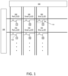
- A display substrate design with a base substrate featuring multiple display units, each with an anode, organic light-emitting layer, and cathode, where cathode lines are connected to driving ICs through insulating layers with strategically placed cathode windows, allowing cathodes to share common windows and reducing the non-display region by arranging display units in a compact manner.


Semiconductor smoothing apparatus and method
PatentActiveUS12119435B2
Innovation
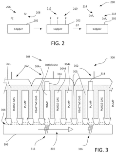
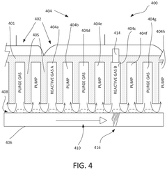
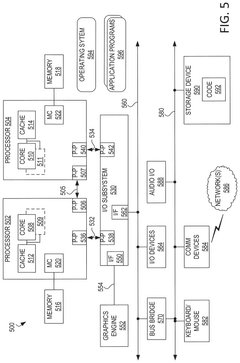
- A semiconductor manufacturing apparatus with discrete open chambers is used to smooth copper surfaces on large substrates, employing reactive plasma or ionic gases to form volatile compounds that are then vaporized and removed, followed by purging, to achieve atomic-level smoothness of copper contact pads, enabling effective bonding between micro-LED elements and the display backplane.
Manufacturing Process Comparison and Scalability Assessment
The manufacturing processes for OLED and MicroLED displays represent fundamentally different approaches to display engineering, with significant implications for scalability and mass production. OLED manufacturing has matured considerably over the past decade, utilizing established vapor deposition techniques for small molecule OLEDs or solution processing for polymer-based variants. These processes occur in highly controlled environments with stringent contamination protocols, as even microscopic particles can cause dead pixels or display irregularities.
OLED production benefits from relatively straightforward layer deposition sequences, though achieving uniform organic layer thickness remains challenging at larger scales. Current manufacturing yields for smartphone-sized OLED panels have reached approximately 85-90% for leading manufacturers, while larger television panels still face yield challenges around 60-70%, contributing to their premium pricing.
In contrast, MicroLED manufacturing presents more complex challenges due to the need for precise placement of millions of microscopic LED chips. The process involves epitaxial growth of LED structures, followed by mass transfer techniques to position individual LEDs onto the display substrate. Current approaches include pick-and-place methods, laser transfer, and fluidic self-assembly, each with distinct advantages and limitations regarding throughput and precision.
MicroLED manufacturing faces a critical bottleneck in the mass transfer process, where placement accuracy must be maintained at micrometer scales across large areas. Current yields for MicroLED displays remain significantly lower than OLED, typically below 40% for prototype production, necessitating extensive repair processes that further increase manufacturing costs.
Regarding scalability, OLED technology demonstrates superior economies of scale for small to medium displays, with established production lines capable of producing millions of smartphone panels annually. However, scaling to larger sizes becomes increasingly challenging due to deposition uniformity issues. MicroLED, while currently less scalable for mass production, theoretically offers better pathways to very large displays through modular assembly approaches.
The equipment investment differs substantially between technologies. OLED requires expensive vacuum chambers and precise deposition systems, with typical fabrication lines costing $5-8 billion. MicroLED manufacturing requires specialized equipment for epitaxial growth and mass transfer, with current estimates suggesting comparable or higher capital expenditure requirements, though with potential for significant reduction as the technology matures.
Energy Efficiency and Environmental Impact Considerations
Energy efficiency represents a critical differentiator between OLED and MicroLED technologies, with significant implications for both consumer experience and environmental sustainability. OLED displays inherently consume less power when displaying darker content due to their emissive nature—pixels can be completely turned off to display true blacks, resulting in substantial energy savings for content with darker scenes. This characteristic makes OLEDs particularly advantageous for mobile devices where battery life is paramount.
MicroLED technology, while still evolving, demonstrates promising energy efficiency potential that may eventually surpass OLED. The inorganic LED materials in MicroLEDs offer higher luminous efficacy, potentially delivering the same brightness levels while consuming less power. This efficiency becomes particularly evident at higher brightness levels, where OLEDs typically require exponentially more power to maintain visibility in bright environments.
From an environmental perspective, the manufacturing processes for both technologies present distinct challenges. OLED production involves organic compounds and solvents that require careful handling and disposal. The shorter lifespan of organic materials also contributes to more frequent device replacement, increasing electronic waste. Conversely, MicroLED manufacturing currently demands more energy-intensive processes and rare earth elements, though these impacts may decrease as production scales and matures.
The carbon footprint of these display technologies extends beyond manufacturing to include operational energy consumption over their lifecycle. For large-format displays like televisions and digital signage, the cumulative energy savings from more efficient technologies can significantly reduce greenhouse gas emissions. Studies indicate that transitioning from conventional LCD to OLED or MicroLED could reduce energy consumption by 20-40% depending on usage patterns and content displayed.
End-of-life considerations also factor into the environmental assessment. The complex material composition of both technologies presents recycling challenges, though MicroLED's inorganic components may offer advantages in material recovery. Several display manufacturers have begun implementing take-back programs and exploring design approaches that facilitate easier disassembly and component separation.
As energy regulations become increasingly stringent worldwide, manufacturers are investing heavily in improving the efficiency of both technologies. Recent advancements include more efficient OLED materials that reduce power consumption by up to 25%, and MicroLED architectures that optimize current distribution to minimize energy loss. These innovations will likely accelerate as energy efficiency becomes an even more prominent market differentiator and regulatory requirement.
Unlock deeper insights with Patsnap Eureka Quick Research — get a full tech report to explore trends and direct your research. Try now!
Generate Your Research Report Instantly with AI Agent
Supercharge your innovation with Patsnap Eureka AI Agent Platform!