Why OLED vs MicroLED Are Revolutionizing Display Interfaces
OCT 24, 202510 MIN READ
Generate Your Research Report Instantly with AI Agent
Patsnap Eureka helps you evaluate technical feasibility & market potential.
OLED and MicroLED Display Evolution Background
Display technology has undergone remarkable evolution since the introduction of cathode ray tubes (CRTs) in the early 20th century. The transition from CRTs to liquid crystal displays (LCDs) marked the first major revolution in display interfaces, enabling thinner, lighter, and more energy-efficient screens. However, the emergence of Organic Light-Emitting Diode (OLED) technology in the late 1990s and early 2000s initiated a new era in display technology, offering superior contrast ratios, wider viewing angles, and the ability to create flexible displays.
OLED technology operates on the principle of electroluminescence, where organic compounds emit light when an electric current passes through them. This fundamental difference from LCD technology—which requires backlighting—allows OLEDs to achieve perfect blacks by simply turning off pixels, resulting in infinite contrast ratios. The commercialization of OLED displays began in the early 2000s, primarily in small devices like mobile phones and digital cameras, before expanding to larger applications such as televisions and monitors.
While OLED technology continued to mature, researchers were simultaneously developing MicroLED technology, which represents the next evolutionary step in display interfaces. MicroLED utilizes inorganic gallium nitride (GaN) LEDs that are microscopic in size—typically less than 100 micrometers. First demonstrated in laboratories in the early 2000s, MicroLED technology combines the self-emissive properties of OLED with the durability and brightness capabilities of inorganic materials.
The technological trajectory of both OLED and MicroLED has been driven by increasing demands for higher resolution, better color accuracy, reduced power consumption, and novel form factors. OLED technology has already achieved significant market penetration, particularly in premium smartphones and high-end televisions, with companies like Samsung and LG leading production innovation. Meanwhile, MicroLED has been positioned as a promising future technology, with companies like Apple, Samsung, and Sony investing heavily in its development.
Recent years have witnessed accelerated advancement in both technologies. OLED has evolved to include variations such as AMOLED (Active-Matrix Organic Light-Emitting Diode) and POLED (Plastic Organic Light-Emitting Diode), enabling applications in foldable smartphones and rollable displays. Concurrently, MicroLED has progressed from laboratory demonstrations to commercial prototypes, with improvements in manufacturing processes gradually reducing production costs.
The convergence of these display technologies with other innovations such as quantum dot enhancement, mini-LED backlighting (as an intermediate step toward MicroLED), and advanced color management systems has further expanded the possibilities for next-generation displays. This technological evolution continues to reshape consumer electronics, automotive interfaces, augmented reality systems, and professional visualization tools.
Market Demand Analysis for Advanced Display Technologies
The advanced display technology market is experiencing unprecedented growth, driven by consumer demand for superior visual experiences across multiple device categories. OLED and MicroLED technologies are at the forefront of this revolution, with the global advanced display market projected to reach $167 billion by 2025, growing at a CAGR of 8.4% from 2020. This growth is primarily fueled by increasing adoption in smartphones, televisions, wearables, and automotive displays.
Consumer preferences are shifting dramatically toward thinner, lighter, and more energy-efficient displays with superior color reproduction and contrast ratios. Market research indicates that 73% of smartphone users consider display quality a critical factor in purchasing decisions, while 65% of TV consumers are willing to pay premium prices for advanced display technologies. This trend is particularly evident in high-end consumer electronics, where OLED has already captured significant market share.
The automotive sector represents one of the fastest-growing segments for advanced displays, with a projected market value of $9.8 billion by 2026. As vehicles become more autonomous and connected, the demand for sophisticated dashboard displays, heads-up displays, and entertainment systems is surging. MicroLED technology is particularly well-positioned for this sector due to its durability and brightness capabilities in varied lighting conditions.
Commercial applications are expanding rapidly as well, with digital signage, retail displays, and corporate environments increasingly adopting these technologies. The commercial display market segment is expected to grow at 12.3% annually through 2025, outpacing consumer segments in percentage growth terms.
Regional analysis reveals that Asia-Pacific dominates manufacturing capacity, while North America and Europe lead in technology innovation and premium market adoption. China's display industry has invested heavily in OLED manufacturing, while South Korean companies maintain leadership in technology development. The North American market shows the highest willingness to adopt cutting-edge MicroLED technology despite its current price premium.
Supply chain constraints present significant challenges, with rare earth materials required for both technologies facing potential shortages. Additionally, manufacturing complexity for MicroLED displays has limited mass production capabilities, creating a supply-demand imbalance that has kept prices elevated. Industry forecasts suggest that manufacturing breakthroughs could reduce MicroLED production costs by 60% within the next five years, potentially accelerating market adoption.
Consumer awareness of display technology differences is growing, with 47% of electronics purchasers now able to identify OLED as a premium display technology, compared to just 18% five years ago. This increased awareness is driving demand for transparent information about display specifications and performance metrics.
Current Technical Challenges in Display Interface Development
Despite significant advancements in display technology, both OLED and MicroLED interfaces face substantial technical challenges that impede their widespread adoption and optimal performance. These challenges represent critical barriers that industry players must overcome to fully realize the revolutionary potential of these technologies.
For OLED displays, manufacturing scalability remains a persistent issue. The production of large OLED panels continues to suffer from low yield rates, particularly for larger screen sizes, resulting in higher costs compared to traditional LCD technology. The complex vapor deposition processes required for OLED manufacturing demand extremely precise control and specialized equipment, creating bottlenecks in production capacity.
Burn-in problems continue to plague OLED technology, especially in applications displaying static content for extended periods. This degradation occurs as organic materials deteriorate at different rates, causing permanent image retention and reducing the display's effective lifespan. While manufacturers have implemented various compensation algorithms, the fundamental material limitation persists.
Blue OLED emitters present a particular challenge, exhibiting shorter lifespans than their red and green counterparts. This differential aging leads to color shift over time, compromising display quality and color accuracy. The search for stable, efficient blue emitters remains an active area of research with significant implications for overall OLED performance.
MicroLED technology faces even more formidable manufacturing hurdles. The mass transfer process—moving millions of tiny LED chips from growth substrates to display backplanes—requires extraordinary precision. Current pick-and-place technologies struggle with the throughput and accuracy needed for cost-effective production at scale, particularly for high-resolution displays requiring smaller LED chips.
Yield management presents another critical challenge for MicroLED. As display resolution increases, the number of individual LED elements grows exponentially, magnifying the impact of defects. Even minimal failure rates can render entire panels unusable, necessitating sophisticated repair mechanisms and redundancy systems that add complexity and cost.
Both technologies confront power efficiency challenges, particularly for mobile applications. While inherently more efficient than LCD, achieving optimal power consumption while maintaining brightness, color accuracy, and refresh rate performance requires sophisticated driving schemes and power management systems that add complexity to display controllers.
Heat dissipation represents another shared challenge, especially for high-brightness applications. Thermal management solutions must be carefully engineered to prevent performance degradation and ensure consistent operation across the entire display surface, adding to design complexity and manufacturing costs.
Addressing these technical challenges requires coordinated efforts across material science, manufacturing engineering, and electronic design disciplines. The industry's ability to overcome these barriers will determine the pace at which these revolutionary display technologies can achieve mainstream adoption across consumer, professional, and industrial applications.
Technical Comparison of OLED vs MicroLED Solutions
01 OLED display structure and fabrication
OLED displays utilize organic light-emitting materials arranged in specific structures to create self-illuminating displays. These displays incorporate multiple layers including cathodes, anodes, and organic emission layers. The fabrication process involves precise deposition of these materials to create efficient light emission. Advanced OLED structures may include specialized pixel arrangements and electrode configurations to enhance brightness, color accuracy, and energy efficiency.- OLED display structure and fabrication: OLED displays utilize organic light-emitting materials arranged in specific structures to create self-illuminating displays. These displays incorporate multiple layers including cathodes, anodes, and organic emission layers. The fabrication processes involve deposition techniques for these various layers to create efficient light emission. OLED technology offers advantages such as high contrast ratios, wide viewing angles, and the ability to create flexible displays.
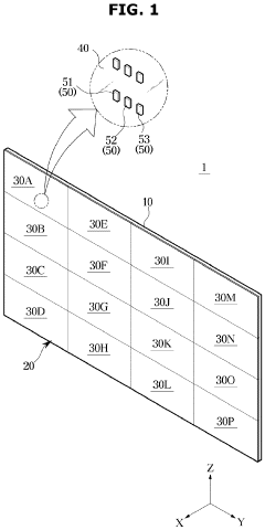
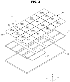
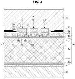
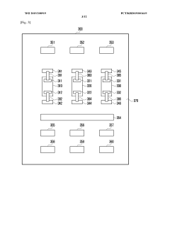
- MicroLED display architecture: MicroLED displays utilize arrays of microscopic LED elements as individual pixel components. These displays feature semiconductor-based inorganic LED structures that are miniaturized and arranged in high-density configurations. The architecture includes transfer and bonding techniques to position the micro-scale LEDs onto display substrates. MicroLED technology offers benefits including high brightness, energy efficiency, and long operational lifetimes.
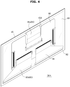
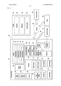
- Display interface technologies: Display interfaces enable communication between display panels and host systems. These interfaces include signal processing circuits, timing controllers, and driver ICs that convert input signals into appropriate display formats. Advanced interfaces support features such as high refresh rates, variable frame rates, and high dynamic range content. The interface technologies also incorporate power management systems to optimize energy consumption while maintaining display performance.
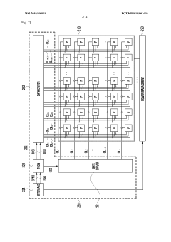
- Pixel driving circuits for advanced displays: Specialized pixel driving circuits are essential for controlling OLED and MicroLED displays. These circuits include thin-film transistor (TFT) backplanes that provide precise current control to each pixel element. Compensation techniques are implemented to address issues like threshold voltage variations and aging effects. Advanced driving schemes enable features such as high dynamic range, wide color gamut, and reduced power consumption through adaptive brightness control.
- Integration of sensors and interactive features: Modern OLED and MicroLED displays increasingly integrate sensors and interactive capabilities directly into the display structure. These include touch sensors, fingerprint readers, and ambient light sensors embedded within the display layers. The integration enables features like under-display cameras, in-display fingerprint recognition, and adaptive brightness control. These technologies require specialized interface protocols to manage the bidirectional flow of information between sensing elements and processing systems.
02 MicroLED display technologies
MicroLED displays utilize arrays of microscopic inorganic LED elements as individual pixels. These displays offer advantages including higher brightness, better energy efficiency, and longer lifespan compared to traditional display technologies. The manufacturing process involves transferring tiny LED chips onto display substrates and establishing electrical connections. MicroLED technology enables high contrast ratios and improved color reproduction for various display applications.Expand Specific Solutions03 Display interface technologies
Display interfaces facilitate communication between display panels and host devices. These interfaces include hardware connections and communication protocols that enable data transfer for image rendering. Modern display interfaces support features such as high refresh rates, increased color depth, and various resolution formats. Advanced interfaces may incorporate features for reduced latency, power management, and compatibility with different display technologies.Expand Specific Solutions04 Pixel driving circuits for OLED and MicroLED
Specialized driving circuits control individual pixels in OLED and MicroLED displays. These circuits regulate current flow to each pixel element to achieve precise brightness levels and color reproduction. Advanced driving architectures may incorporate compensation mechanisms for uniform display performance and extended operational life. The driving circuits are designed to address challenges such as pixel aging, temperature variations, and power efficiency requirements.Expand Specific Solutions05 Integration of display technologies with device systems
OLED and MicroLED displays are integrated into various electronic devices through specialized system architectures. This integration involves hardware and software components that enable displays to function within larger device ecosystems. System-level considerations include power management, thermal control, and signal processing optimizations. Advanced integration approaches may incorporate features for adaptive brightness, reduced blue light emission, and enhanced user interaction capabilities.Expand Specific Solutions
Key Industry Players in Next-Generation Display Manufacturing
The OLED vs MicroLED display technology market is currently in a transitional phase, with OLED reaching maturity while MicroLED remains in early commercialization. The global advanced display market is projected to exceed $200 billion by 2025, driven by increasing demand for high-performance screens in consumer electronics and automotive applications. BOE Technology Group and Samsung Electronics lead OLED production with established manufacturing capabilities, while companies like Lumileds and Applied Materials are advancing MicroLED development. Chinese manufacturers including China Star Optoelectronics are rapidly expanding capacity to challenge Korean dominance. Meanwhile, specialized players such as OLEDWorks and eMagin focus on niche applications. The competitive landscape is characterized by intense patent activity and strategic partnerships as companies position themselves in this high-growth sector where display technologies are converging with AI and IoT applications.
BOE Technology Group Co., Ltd.
Technical Solution: BOE has developed comprehensive solutions in both OLED and MicroLED technologies. Their OLED technology includes flexible AMOLED displays with integrated touch functionality (On-Cell Touch AMOLED) that achieves thickness reduction of approximately 20% compared to traditional structures[1]. BOE's OLED panels feature pixel densities exceeding 500 PPI with HDR10+ certification, achieving peak brightness of 1,500 nits while maintaining power efficiency. For MicroLED, BOE employs a hybrid integration approach combining PCB substrates with TFT backplanes, allowing for displays with pixel pitches as small as 0.9mm[2]. Their Active Matrix MicroLED technology utilizes proprietary mass transfer processes to achieve placement accuracy within ±1.5μm, enabling high-yield manufacturing. BOE has demonstrated 75-inch 8K MicroLED prototypes with brightness exceeding 1,000 nits and a color gamut covering 114% of DCI-P3[3].
Strengths: Extensive manufacturing infrastructure with multiple production lines; strong R&D capabilities with over 10,000 display patents; vertical integration from panel to module assembly. Weaknesses: Still catching up to Samsung and LG in OLED manufacturing yield rates; MicroLED mass production capabilities remain limited compared to more established display technologies.
Samsung Electronics Co., Ltd.
Technical Solution: Samsung has pioneered both OLED and MicroLED technologies with significant market presence. For OLED, Samsung utilizes its proprietary AMOLED technology in mobile displays and QD-OLED for larger panels, achieving superior color accuracy with 100% DCI-P3 coverage and response times as low as 0.1ms[1]. Their MicroLED solution employs inorganic gallium nitride-based LEDs at microscopic scale (under 50 micrometers), enabling modular, bezel-free displays with brightness exceeding 2,000 nits while maintaining perfect blacks[2]. Samsung's The Wall represents their commercial MicroLED implementation, featuring self-emissive pixels with individual RGB subpixels that eliminate the need for color filters, resulting in exceptional contrast ratios and color volume. Their manufacturing process involves advanced mass transfer techniques to place millions of MicroLEDs precisely onto substrates[3].
Strengths: Vertical integration from semiconductor manufacturing to display production; established mass production capabilities for both technologies; proprietary quantum dot enhancement for color performance. Weaknesses: High manufacturing costs for MicroLED with current yield challenges; OLED technology still faces burn-in issues and shorter lifespan compared to traditional LCD displays.
Breakthrough Patents and Research in Display Interface Technology
Display device comprising display module, and manufacturing method therefor
PatentPendingEP4401159A1
Innovation
- The display apparatus incorporates a substrate with inorganic light-emitting diodes, a front cover, a metal plate, a side cover, and a side end member with ribs for enhanced conductivity and sealing, which improves electrostatic discharge protection and reduces gaps between modules, making the display apparatus more robust and visually seamless.
LED display and electronic device having same
PatentWO2019208919A1
Innovation
- The development of a micro-LED display with a bezel-less design and segmentation capabilities, allowing for flexible displays of various sizes, achieved through direct mounting of micro-LEDs on a substrate and innovative electrical connections using conductive patterns and wiring lines, enabling robust electrical connections and flexible display configurations.
Energy Efficiency and Sustainability Considerations
Energy efficiency represents a critical differentiator between OLED and MicroLED technologies, with significant implications for both consumer experience and environmental impact. OLED displays inherently consume less power when displaying darker content due to their emissive nature, where black pixels are simply turned off. This pixel-level power management enables OLEDs to achieve up to 40% energy savings compared to traditional LCD displays in real-world usage scenarios with mixed content.
MicroLED technology, while still evolving, demonstrates promising efficiency characteristics that may eventually surpass OLED. Current prototypes show 30-50% higher luminous efficacy than comparable OLED panels, translating to more light output per watt consumed. This efficiency advantage becomes particularly significant in high-brightness applications such as outdoor displays or automotive interfaces where power demands are substantial.
From a manufacturing sustainability perspective, both technologies present distinct environmental considerations. OLED production involves fewer process steps and lower temperature requirements than traditional LCD manufacturing, reducing overall energy consumption during fabrication. However, certain OLED materials contain rare elements with limited global supplies, raising concerns about long-term resource availability and extraction impacts.
MicroLED manufacturing currently demands precision assembly techniques that are energy-intensive, though rapid advances in mass transfer technologies are steadily improving production efficiency. The exceptional longevity of MicroLED displays—with theoretical lifespans exceeding 100,000 hours without significant degradation—contributes positively to sustainability by reducing replacement frequency and electronic waste generation.
End-of-life considerations reveal additional sustainability factors. OLED panels contain organic compounds that may require specialized recycling processes, while MicroLED displays primarily comprise inorganic materials that potentially offer simpler recycling pathways. Both technologies are driving innovations in circular design approaches, with manufacturers increasingly incorporating modular components and recyclable materials to address growing regulatory and consumer demands for sustainable electronics.
Power management innovations continue to enhance the efficiency profiles of both technologies. Advanced pixel compensation algorithms, adaptive refresh rates, and intelligent brightness controls are being implemented across both OLED and MicroLED platforms, further reducing energy consumption while maintaining optimal visual performance across diverse usage scenarios and environmental conditions.
Supply Chain and Manufacturing Process Analysis
The supply chain for OLED and MicroLED technologies represents a complex ecosystem with distinct manufacturing challenges and opportunities. OLED production has matured significantly over the past decade, with established supply chains dominated by South Korean manufacturers like Samsung and LG Display, alongside emerging Chinese competitors. The manufacturing process involves depositing organic materials onto substrates through techniques such as vacuum thermal evaporation, with subsequent encapsulation to protect against moisture and oxygen degradation.
Material sourcing for OLED production presents ongoing challenges, particularly regarding rare elements used in phosphorescent materials. The supply chain remains vulnerable to disruptions in these specialized chemical components, though recent advancements in material science have introduced more sustainable alternatives. Production yields have improved substantially, with modern facilities achieving approximately 85-90% yield rates for mobile displays, though larger panels still face yield challenges.
MicroLED manufacturing, by contrast, exists in a nascent state with fragmented supply chains still under development. The process involves transferring millions of microscopic LED chips from epitaxial wafers to display substrates—a procedure requiring unprecedented precision. This mass transfer process represents the primary manufacturing bottleneck, with current technologies struggling to achieve economically viable throughput rates for consumer applications.
The semiconductor materials required for MicroLED production leverage existing supply chains from the LED industry, though with significantly higher quality and uniformity requirements. Silicon backplanes utilize established semiconductor fabrication infrastructure, creating potential integration opportunities with existing chip manufacturers. However, the specialized equipment needed for precise chip transfer and placement remains limited to a few equipment vendors globally.
Cost structures differ dramatically between these technologies. OLED manufacturing has benefited from economies of scale, with production costs decreasing approximately 15% annually over recent years. MicroLED production costs remain prohibitively high for mass-market applications, with estimates suggesting current costs at 5-10 times that of equivalent OLED displays, primarily due to low yields and complex assembly processes.
Environmental considerations also differentiate these supply chains. OLED manufacturing involves hazardous organic solvents requiring careful handling and disposal, while MicroLED production generally utilizes more conventional semiconductor processes with established environmental controls. Both technologies face sustainability challenges regarding rare material usage, though MicroLED potentially offers advantages through longer device lifespans and more recyclable components.
Unlock deeper insights with Patsnap Eureka Quick Research — get a full tech report to explore trends and direct your research. Try now!
Generate Your Research Report Instantly with AI Agent
Supercharge your innovation with Patsnap Eureka AI Agent Platform!