Display apparatus and manufacturing method therefor, and active matrix circuit board

A technology for a display device and a manufacturing method, applied to identification devices, static indicators, instruments, etc., capable of solving problems such as deterioration of display quality

Inactive Publication Date: 2014-07-23
SHARP KK
View PDF9 Cites 0 Cited by
  • Summary
  • Abstract
  • Description
  • Claims
  • Application Information

AI Technical Summary

Problems solved by technology

Therefore, in the liquid crystal display device including this active matrix substrate, there is a problem that when a disconnection occurs in the display wiring of the gate line and the source line, in the disconnected display wiring, The signal for display from the drive circuit is not supplied to the rear from this disconnection position, so the display quality deteriorates significantly

Method used


Image

  • Display apparatus and manufacturing method therefor, and active matrix circuit board
  • Display apparatus and manufacturing method therefor, and active matrix circuit board
  • Display apparatus and manufacturing method therefor, and active matrix circuit board

Examples


Embodiment approach 1

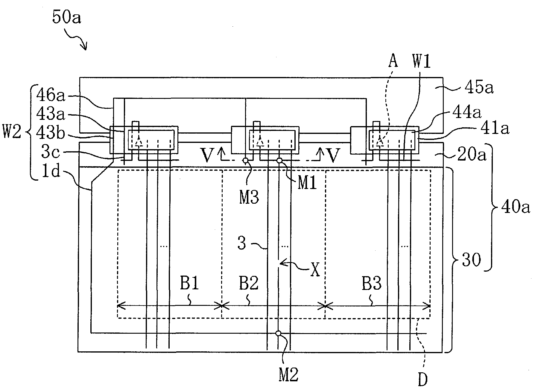
[0065] Figure 1 to Figure 5 Embodiment 1 of the display device, its manufacturing method, and active matrix substrate of the present invention is shown.

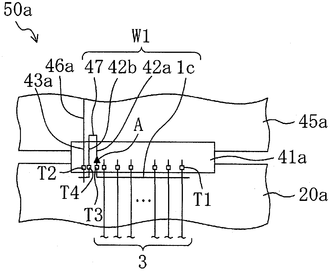
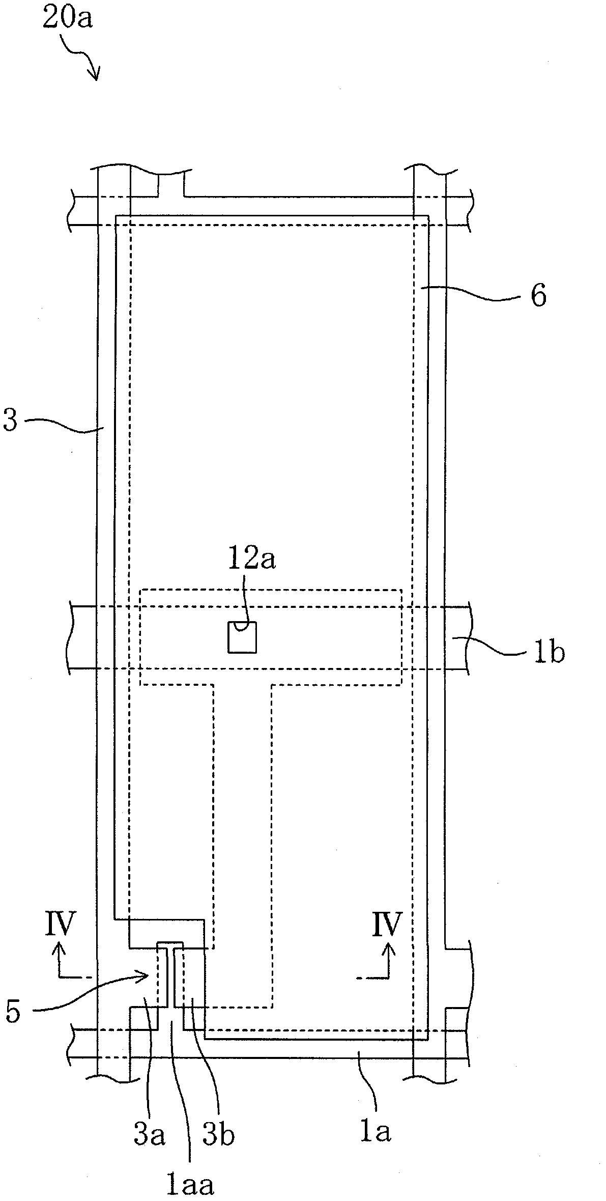
[0066] Specifically, figure 1 It is a plan view of the liquid crystal display device 50a of this embodiment, figure 2 It is an enlarged plan view of the film substrate 41a constituting the liquid crystal display device 50a and its surroundings. in addition, image 3 is a plan view showing one pixel of the active matrix substrate 20a constituting the liquid crystal display device 50a, Figure 4 is along image 3 The cross-sectional view of the active matrix substrate 20a and the liquid crystal display panel 40a equipped with it on the line IV-IV in FIG. and, Figure 5 is along figure 1 A cross-sectional view of the active matrix substrate 20a taken along line V-V in FIG.

[0067] Such as figure 1 As shown, the liquid crystal display device 50a includes: a liquid crystal display panel 40a; three film substrates 4...

Embodiment approach 2

[0123] Image 6 It is an enlarged plan view of the film substrate 41b constituting the liquid crystal display device 50b of this embodiment and its surroundings. In addition, in the following embodiments, for the Figure 1 to Figure 5 The same reference numerals are attached to the same parts, and detailed description thereof will be omitted.

[0124] In Embodiment 1 above, one first wiring W1 and one amplifier circuit A are provided for each film substrate 41a, but in this embodiment, as Image 6 As shown, two first wirings W1 and amplifier circuits A are provided for each film substrate 41b.

[0125] Specifically, as Image 6 As shown, in the active matrix substrate 20b (liquid crystal display panel 40b) constituting the liquid crystal display device 50b of this embodiment, the plurality of source lines 3 in the blocks B1 to B3 constitute two wiring groups G1 and G2. and, if Image 6 As shown, in the liquid crystal display device 50b, the first wiring W1 and the amplifi...

Embodiment approach 3

[0128] Figure 7 It is a plan view of the liquid crystal display device 50c of this embodiment.

[0129] In Embodiments 1 and 2 above, the source driver 44a is provided on the film substrates 41a and 41b, respectively, but in this embodiment, the source driver 35a is provided on the liquid crystal display panel 40c (active matrix substrate 20c).

[0130] Such as Figure 7 As shown, the liquid crystal display device 50c includes a liquid crystal display panel 40c and a film substrate 45c attached to the upper end of the liquid crystal display panel 40c in the figure via an ACF (not shown).

[0131] Such as Figure 7 As shown, the liquid crystal display panel 40c includes an active matrix substrate 20c and a counter substrate 30 arranged to face each other.

[0132] In the active matrix substrate 20c, the structure of the display region D is substantially the same as that of the active matrix substrate 20a in Embodiment 1, as shown in Figure 7 As shown, on the outside of th...


PUM

PropertyMeasurementUnit
thicknessaaaaaaaaaa

Abstract

A display panel includes a plurality of display lines provided in each of blocks and extending in parallel with each other, a plurality of drive circuits provided outside a display region and connected to the display lines in the respective blocks, a plurality of first lines provided outside the display region and intersecting end portions closer to the drive circuits of the display lines in the respective blocks, the first lines being insulated from the display lines, and a second line provided outside the display region and intersecting end portions farther from the drive circuits of the display lines of all the blocks, the second line being insulated from the display lines. The second line is configured to intersect the first lines while being insulated from the first lines, and be supplied with a display signal from each of the drive circuits via an amplifier circuit.

Description

technical field [0001] The present invention relates to a display device, a method for manufacturing the same, and an active matrix substrate, and particularly relates to a technique for correcting disconnection of display wiring disposed on the active matrix substrate and the display device. Background technique [0002] A liquid crystal display device includes, for example, an active matrix substrate and a counter substrate arranged to face each other. This active matrix substrate includes, for example, a plurality of gate lines extending parallel to each other and a plurality of source lines extending parallel to each other in a direction perpendicular to each gate line as display wiring. Therefore, in the liquid crystal display device including this active matrix substrate, there is a problem that when a disconnection occurs in the display wiring of the gate line and the source line, in the disconnected display wiring, Since the signal for display from the drive circuit...

Claims


Application Information

Patent Timeline
Patent Type & Authority Patents(China)
IPC IPC(8): G09F9/30G02F1/13G02F1/1345G02F1/1368G09F9/00
CPCG09G2330/08G09G3/006G09G3/3611G02F2001/136272G02F2001/133388G02F2001/136263G09G2300/0426G02F1/136259Y10T29/49004G02F1/133388G02F1/136263G02F1/136272
Inventor 尾关忠敏山田崇晴吉田昌弘光本一顺
Owner SHARP KK
Why Eureka
Try Eureka