Method for generating interface frameworks of semiconductor software

A software interface and interface frame technology, applied in the direction of program control devices, etc., can solve the problems of software interface layer confusion, inconsistent interface style, unfavorable function realization, etc., achieve the effect of clear hierarchical structure and improve design efficiency

Inactive Publication Date: 2012-07-04
BEIJING SEVENSTAR ELECTRONICS CO LTD
View PDF4 Cites 13 Cited by
  • Summary
  • Abstract
  • Description
  • Claims
  • Application Information

AI Technical Summary

Problems solved by technology

[0002] At present, the interface design of software in the semiconductor process equipment manufacturing industry usually adopts a block layout, which is independently designed according to functional modules, and the realization of each sub-interface requires repeated layout design, which leads to confusion in the software interface hierarchy and low efficiency in the implementation process , and the interface style is not uniform, which has a certain degree of disadvantage and influence on the overall structure of the software and the realization of subsequent functions

Method used


Image

  • Method for generating interface frameworks of semiconductor software
  • Method for generating interface frameworks of semiconductor software

Examples


Embodiment Construction

[0021] The specific implementation manners of the present invention will be further described in detail below in conjunction with the accompanying drawings and embodiments. The following examples are used to illustrate the present invention, but are not intended to limit the scope of the present invention.

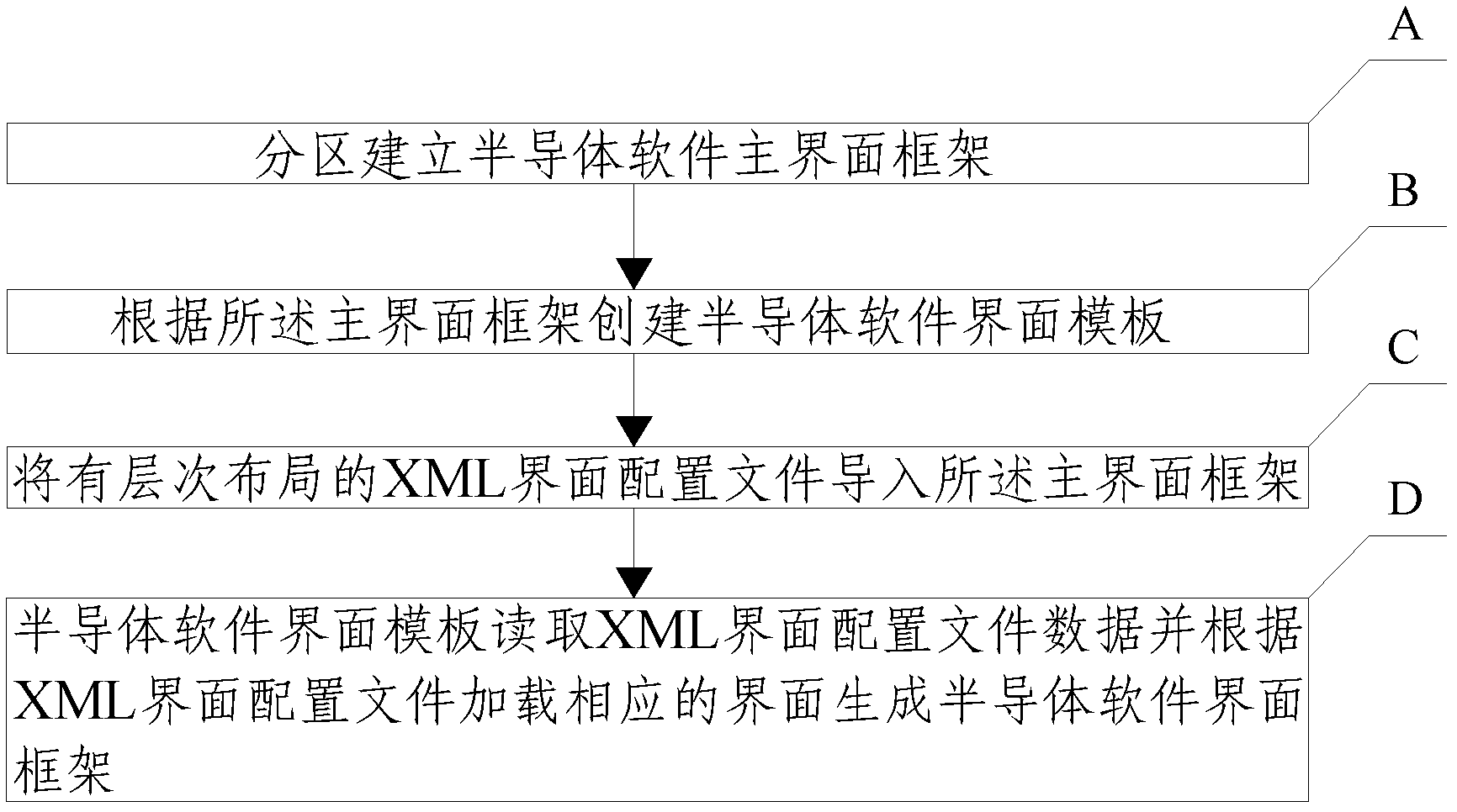
[0022] like figure 1 As shown, the semiconductor software interface frame generation method described in the present invention comprises the following steps:

[0023] A: Partition to establish the main interface framework of semiconductor software;

[0024] In this step, the title area, information area, and navigation area of ​​the interface frame are established, and according to the layering of the XML interface configuration file, the partitions of the semiconductor software interface frame are one-to-one corresponding to the hierarchical structure of the XML interface configuration file. Among them, the title area is mainly a fixed area, which mainly displays inform...


PUM


Abstract

The invention discloses a method for generating interface frameworks of semiconductor software, which relates to the technical field of software design. The method for generating the interface frameworks of the semiconductor software comprises the following steps: A-, establishing main interface frameworks of the semiconductor software in the manner of partition; B-, creating interface templates of the semiconductor software according to the main interface frameworks; C-, respectively importing extensive makeup language (XML) interface configuration files with hierarchical layouts into the main interface frameworks; and D-, reading the data of the XML interface configuration files by the interface templates of the semiconductor software, and loading corresponding interfaces according to the XML interface configuration files to generate the interface frameworks of the semiconductor software. According to the method for generating the interface frameworks of the semiconductor software, the unified layout of functional elements of semiconductor software interfaces is realized; implementation and call on the software interfaces can be performed by a user interface through a unified method; users realize grouping display control of the interfaces through modifying the configuration files; the interfaces respectively have a clear hierarchical structure; the number of the interfaces can be increased or reduced through modifying the configuration files without modifying source codes, thereby, the design efficiency of the semiconductor software interfaces is increased, and convenience in brought to the users.

Description

technical field [0001] The invention relates to the technical field of software design, in particular to a method for generating a semiconductor software interface frame. Background technique [0002] At present, the interface design of software in the semiconductor process equipment manufacturing industry usually adopts a block layout, which is independently designed according to functional modules, and the realization of each sub-interface requires repeated layout design, which leads to confusion in the software interface hierarchy and low efficiency in the implementation process , and the interface style is not uniform, which has a certain degree of disadvantage and influence on the overall structure of the software and the realization of subsequent functions. Contents of the invention [0003] (1) Technical problems to be solved [0004] The technical problem to be solved by the present invention is to provide a semiconductor software interface frame generation method...

Claims


Application Information

Patent Timeline
Patent Type & Authority Applications(China)
IPC IPC(8): G06F9/44
Inventor 王春洪周法福钟结实黄扬君
Owner BEIJING SEVENSTAR ELECTRONICS CO LTD
Why Eureka
Try Eureka