Channel type power metal oxide semi-conductor structure with fast switching capacity and manufacture method

A technology of fast switching and manufacturing methods, applied in semiconductor/solid-state device manufacturing, semiconductor devices, electrical components, etc., can solve the problem of increased power loss, affecting the switching speed of power metal oxide half field effect transistors, power metal oxide half field effect transistors Issues such as limited reverse recovery ability

CN102751190BInactive Publication Date: 2014-12-03SUPER GROUP SEMICON
6 Cites 0 Cited by

Patent Information

Authority / Receiving Office
CN · China
Patent Type
Patents(China)
Current Assignee / Owner
Publication Date
2014-12-03
Estimated Expiration
Not applicable · inactive patent

Smart Images

  • Figure 1
    Figure 1
  • Figure 2
    Figure 2
  • Figure 3
    Figure 3
Patent Text Reader

Abstract

Provided are a channel type power metal oxide semi-conductor structure with fast switching capacity and a manufacture method. The method includes the following steps: first, forming an epitaxial layer of a first electric conducting type on a substrate, and then, forming a plurality of gate structures in the epitaxial layer; forming a shallow doping area with the first electric conducting type on the surface of the epitaxial layer, and then forming a shielding structure on the shallow doping area; forming a plurality of well areas with a second electric conducting type in the epitaxial layer by using the shielding structure, and then forming a source doping area with the first electric conducting type on the surface of the well areas; doping concentration of the shallow doping area is smaller than that of the source doping area and the well areas, and the doping concentration of the shallow doping area is larger than that of the epitaxial layer. The channel type power metal oxide semi-conductor structure with the fast switching capacity and the manufacture method can effectively reduce forward voltage drop (VSD) of a source drain diode and obtain channel type power semi-conductors with the fast switching capacity and low switching power loss.
Need to check novelty before this filing date? Find Prior Art

Description

technical field

[0001] The invention relates to a trench type power metal oxide semiconductor structure and a manufacturing method thereof, in particular to a power metal oxide semiconductor structure with fast switching capability and a manufacturing method thereof. Background technique

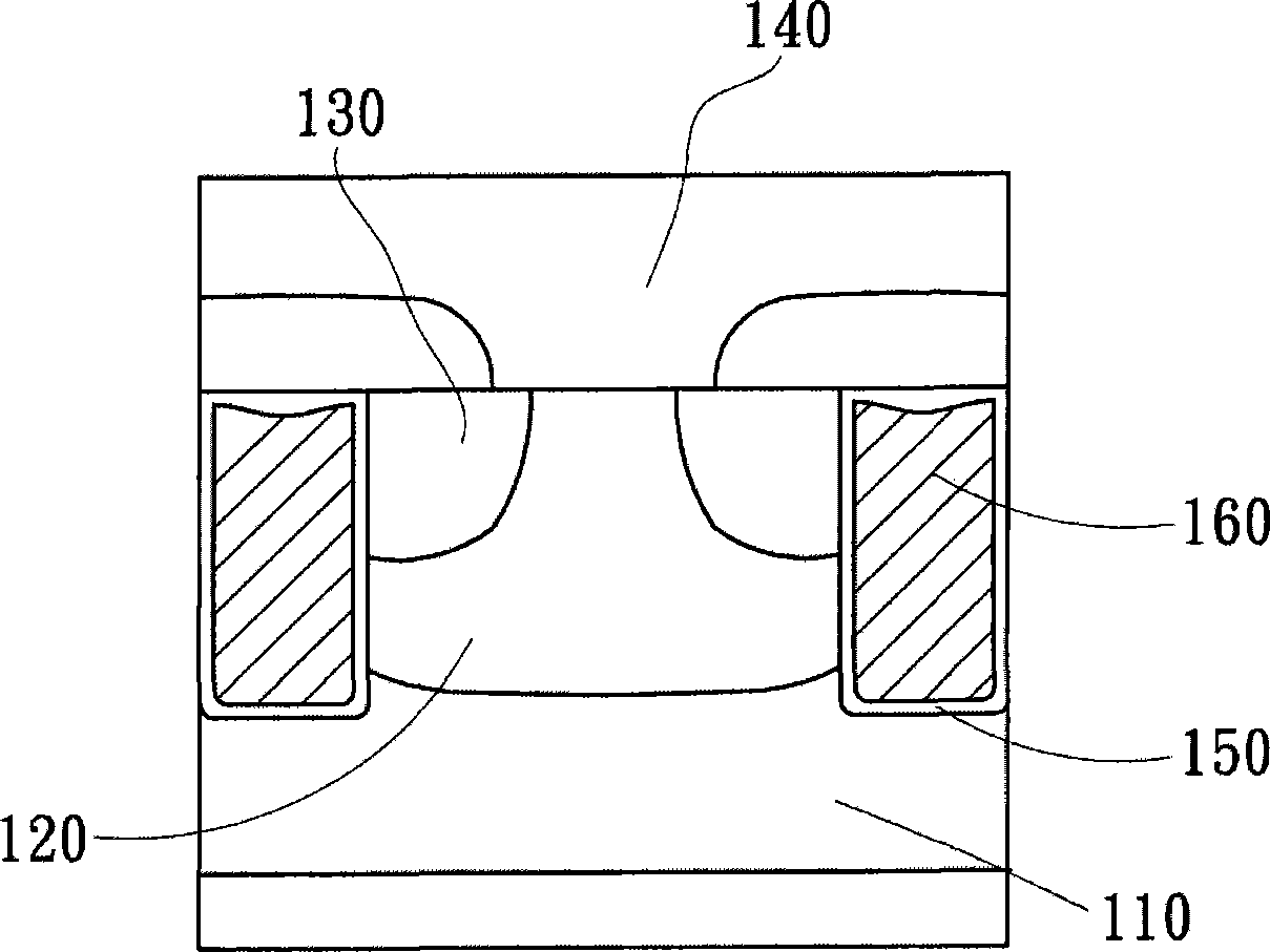
[0002] In the application field of trench power metal oxide semiconductors, the performance of switching speed has been paid more and more attention. The improvement of this characteristic can significantly improve the power loss during switching in high frequency circuit operation. figure 1 It is a cross-sectional view of a traditional n-channel gate trench power metal oxide half field effect transistor (MOSFET). The structure is composed of an n-type drain region 110 , a p-type body region 120 , an n-type source region 130 , a metal layer 140 connected to the source electrode, a gate oxide layer 150 and a gate compound crystal structure 160 .

[0003] When the metal oxide semiconductor ...

Examples

Embodiment Construction

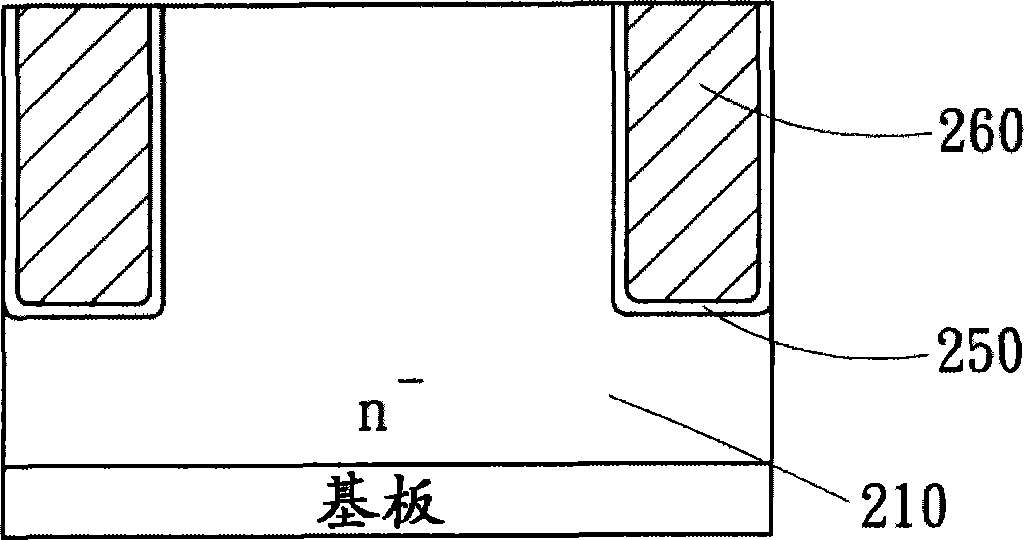
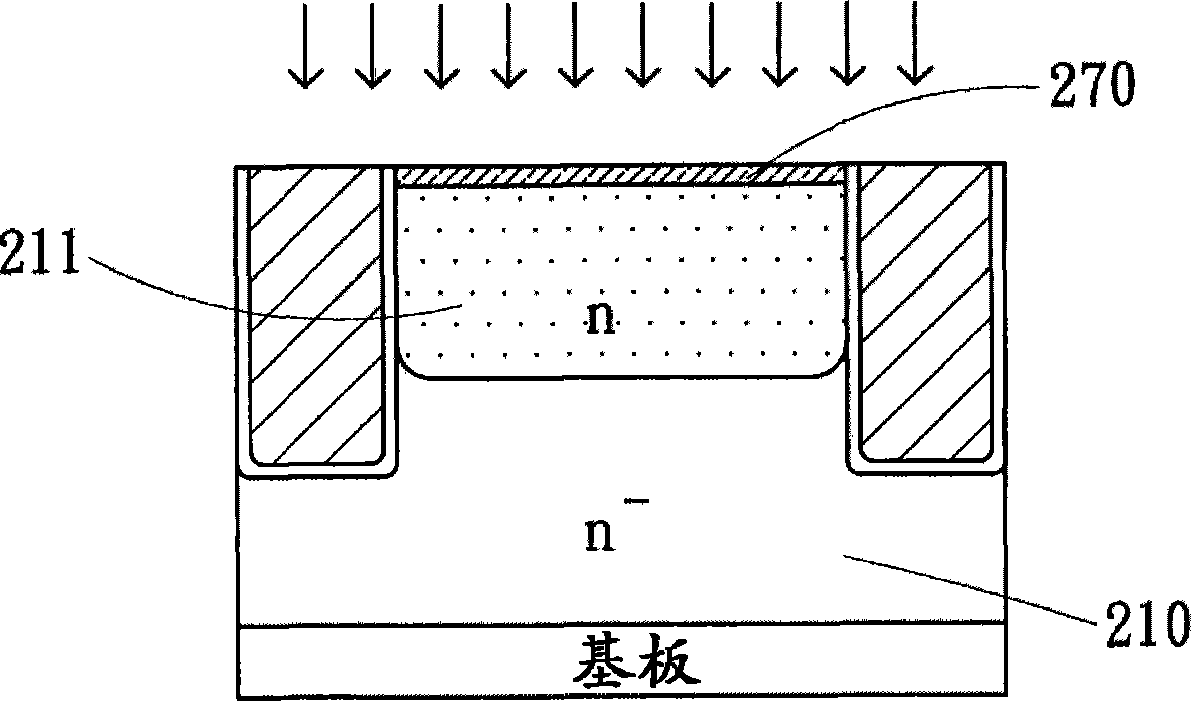
[0039] The main technical feature of the present invention is to form a shallow doped region of the same conductivity type as the source doped region between adjacent wells. When the power MOSFET turns from on to off, the shallow doped region can provide a path for the reverse current, so that the forward voltage drop of the source-drain diode (V SD ) is reduced to about 0.1 volts to 0.2 volts. In this way, the reverse current can quickly remove the excessive minority carriers at the junction, greatly improving the reverse recovery (Reverse Recovery) capability of the power metal oxide half field effect transistor. When the transistor is switched, excessive power loss is avoided. The structure of the present invention can avoid affecting the withstand voltage characteristics and breakdown voltage (BVDSS) of the gate oxide layer, and obtain a power metal oxide semiconductor field effect transistor with high reliability and fast switching capability.

[0040] Figure 2A to Fig...