
Touch panel and touch display panel
A touch display panel, touch panel technology, applied in the direction of instruments, electrical digital data processing, digital data processing components, etc., can solve the problems of inability to combine aesthetics, and achieve the effect of improving aesthetics and matching
- Summary
- Abstract
- Description
- Claims
- Application Information
AI Technical Summary
Problems solved by technology
Method used
Image

Examples
Embodiment Construction
[0023] In order to enable those who are familiar with the technical field of the present invention to further understand the present invention, the preferred embodiments of the present invention are enumerated below, together with the accompanying drawings, to describe in detail the composition of the present invention and the desired effect .
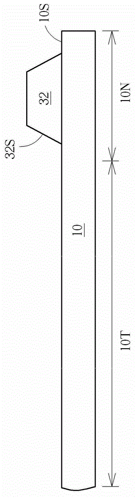
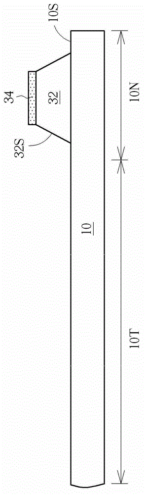
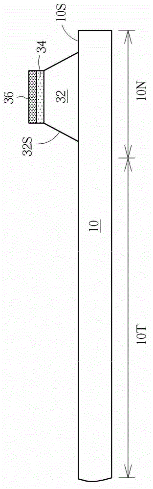
[0024] Please refer to Figure 1 to Figure 8 . Figure 1 to Figure 8 A schematic diagram of a method for manufacturing a touch panel according to a first embodiment of the present invention is shown. Such as figure 1 As shown, a substrate 10 is provided first. The substrate 10 can be a transparent substrate such as a glass substrate or a plastic substrate. The substrate 10 has a transparent region 10T and an opaque region 10N. The opaque region 10N can be located on one side, two sides, three sides of the transparent region 10T or surround the transparent region 10T. Next, a white semi-transparent pattern 32 is formed in the opaqu...
PUM
 Abstract
Description
Claims
Application Information