Display device and pixel unit defect repairing method thereof

A display device and a pixel unit technology, applied in the field of OLED display, can solve the problems of ineffective repair and increase of pixel defects in the manufacturing process, etc.

Active Publication Date: 2014-05-21
GUANGDONG JUHUA PRINTING DISPLAY TECH CO LTD
View PDF6 Cites 39 Cited by
  • Summary
  • Abstract
  • Description
  • Claims
  • Application Information

AI Technical Summary

Problems solved by technology

This solution will increase the manufacturing process and can only solve pixel defects caused by transistor failures, and cannot effectively repair defects caused by failures in other parts of the drive circuit

Method used


Image

  • Display device and pixel unit defect repairing method thereof
  • Display device and pixel unit defect repairing method thereof
  • Display device and pixel unit defect repairing method thereof

Examples


Embodiment Construction

[0030] The technical solutions of the present invention will be further described below in conjunction with the accompanying drawings and through specific implementation methods.

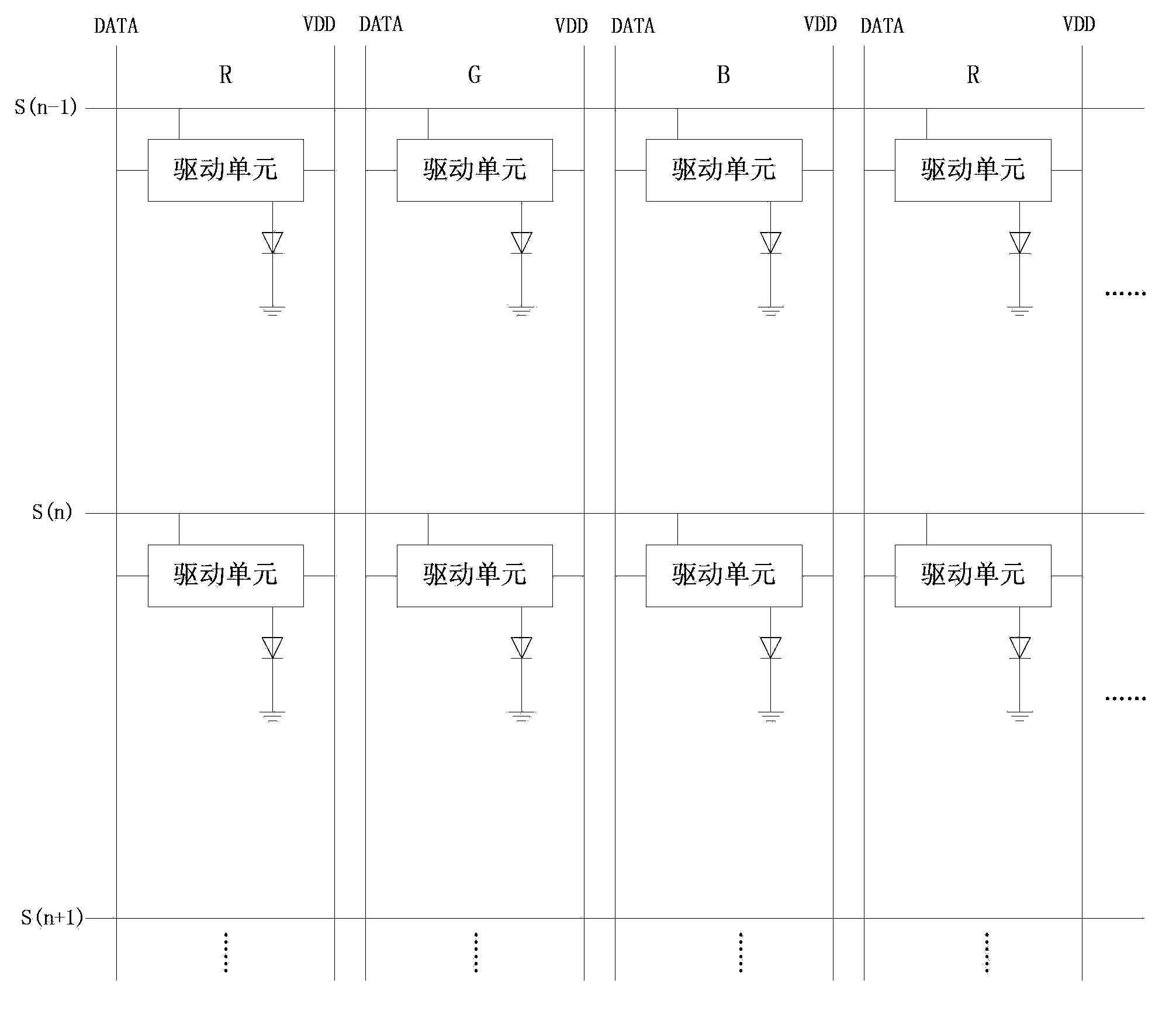
[0031] figure 2 It is a schematic structural diagram of a display device provided in Embodiment 1 of the present invention. The display device includes scan lines, data lines, and pixel units. Each pixel unit includes a drive unit and an organic light-emitting device. The output terminal of the drive circuit is connected to the organic light-emitting device. connected to the input terminal for driving the organic light emitting diode for lighting.

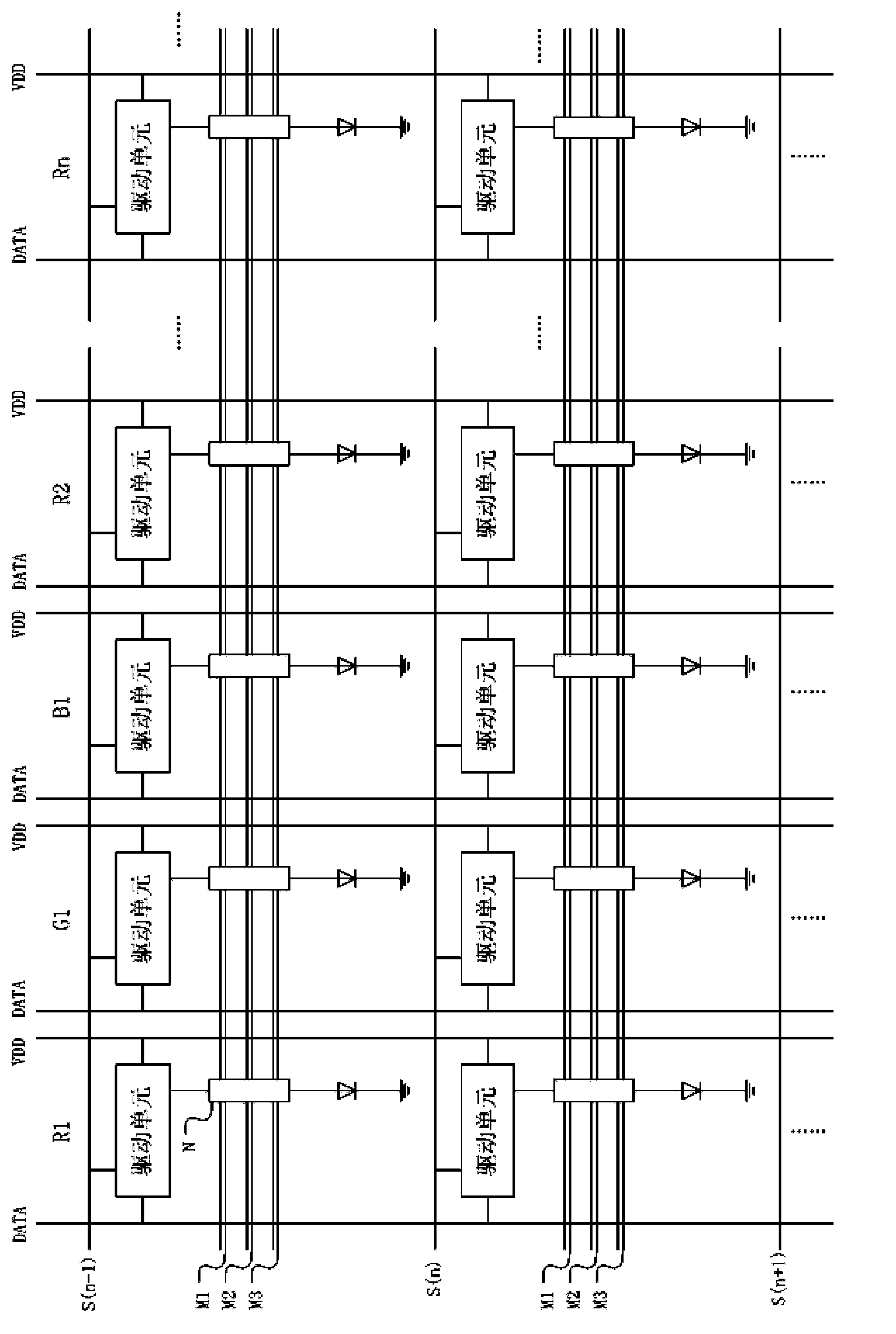
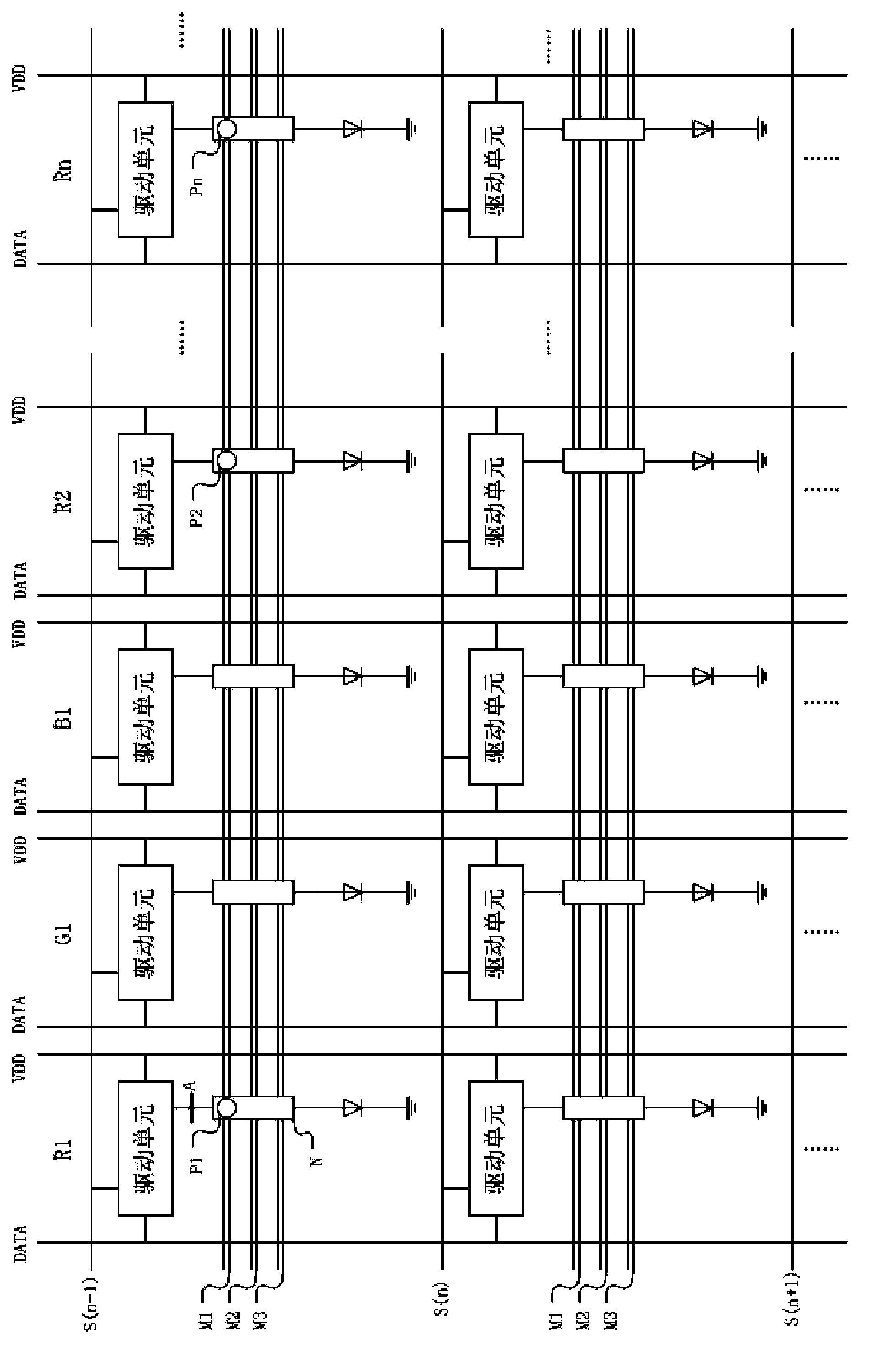
[0032] In the display device, repair lines M1 , M2 and M3 are arranged along the scanning line direction, and the repair lines are arranged through a mask plate by using a light-shielding layer metal above the substrate. A metal bridging region N is arranged above the repair line, and the metal bridging region is arranged on a gate metal layer, which i...


PUM


Abstract

The invention discloses a display device and a pixel unit defect repairing method thereof. The display device comprises a scanning line, a data line, a pixel unit, wherein the scanning line and the data line are arranged on a substrate and are mutually intersected; and the pixel unit includes a drive circuit and an organic light-emitting device. Besides, a light shield layer arranged above the substrate is provided with a repairing line along the data line or scanning line direction; a metal bridging zone is arranged above the repairing line; and the repairing line and the metal bridging zone are used for breaking the drive circuit of the fault pixel unit and connecting a drive signal of a normal homochromic pixel unit. According to the invention, on the basis of unchanging of a mask plate, the reserved repairing line is made by using the light shield layer and a gate metal layer and an organic light-emitting device with a fault drive circuit is connected in parallel with an organic light-emitting device of a normal homochromic pixel unit, so that the pixel defect of the point becomes less obvious and thus a pixel defect caused by any drive circuit fault can be overcome.

Description

technical field [0001] The invention relates to the technical field of OLED display, in particular to a defect repairing method of a display device and a pixel unit thereof. Background technique [0002] The display panel is composed of many display points, and the liquid crystal material on each display point changes the amount of light transmission under the control of electrical signals for imaging. For example, there are 786,432 display points in a display panel with a resolution of 1024×768. On the side of the display panel array substrate, each display point corresponds to three pixels; on the side of the display panel color filter film substrate, respectively Corresponding to three kinds of filter units of red R, green G and blue B, each filter unit corresponds to a pixel. Any problem with the dots in the display panel and the structure of the driving part and backlight part corresponding to these dots will make this pixel a point defect, and a point defect is an irr...

Claims


Application Information

Patent Timeline
Patent Type & Authority Applications(China)
IPC IPC(8): G09G3/32G09G3/3225
CPCG09G3/3225G09G2300/0426G09G2330/08G09G2330/10
Inventor 蔡韬田凯郭峰
Owner GUANGDONG JUHUA PRINTING DISPLAY TECH CO LTD
Why Eureka
Try Eureka