Lighting inspection device of organic EL display substrate and method thereof

A technology for lighting inspection and display panels, which is applied to instruments, electric solid-state devices, semiconductor devices, etc., can solve the problems of time-consuming and difficult to realize automation, and achieve the effect of ensuring luminous life.

Inactive Publication Date: 2011-08-31
HITACHI HIGH-TECH CORP
View PDF6 Cites 15 Cited by
  • Summary
  • Abstract
  • Description
  • Claims
  • Application Information

AI Technical Summary

Problems solved by technology

That is, defective pixel inspection is performed in units of panels, so inspection devices and inspection jigs corresponding to various product sizes are required, and it is difficult to automate to improve productivity
In addition, since there is no production line, when detecting defective pixels, it takes time to feed back the results of the image quality inspection performed at the same time to the previous process, and it takes time to take measures to improve the pass rate

Method used


Image

  • Lighting inspection device of organic EL display substrate and method thereof
  • Lighting inspection device of organic EL display substrate and method thereof
  • Lighting inspection device of organic EL display substrate and method thereof

Examples


Embodiment 1

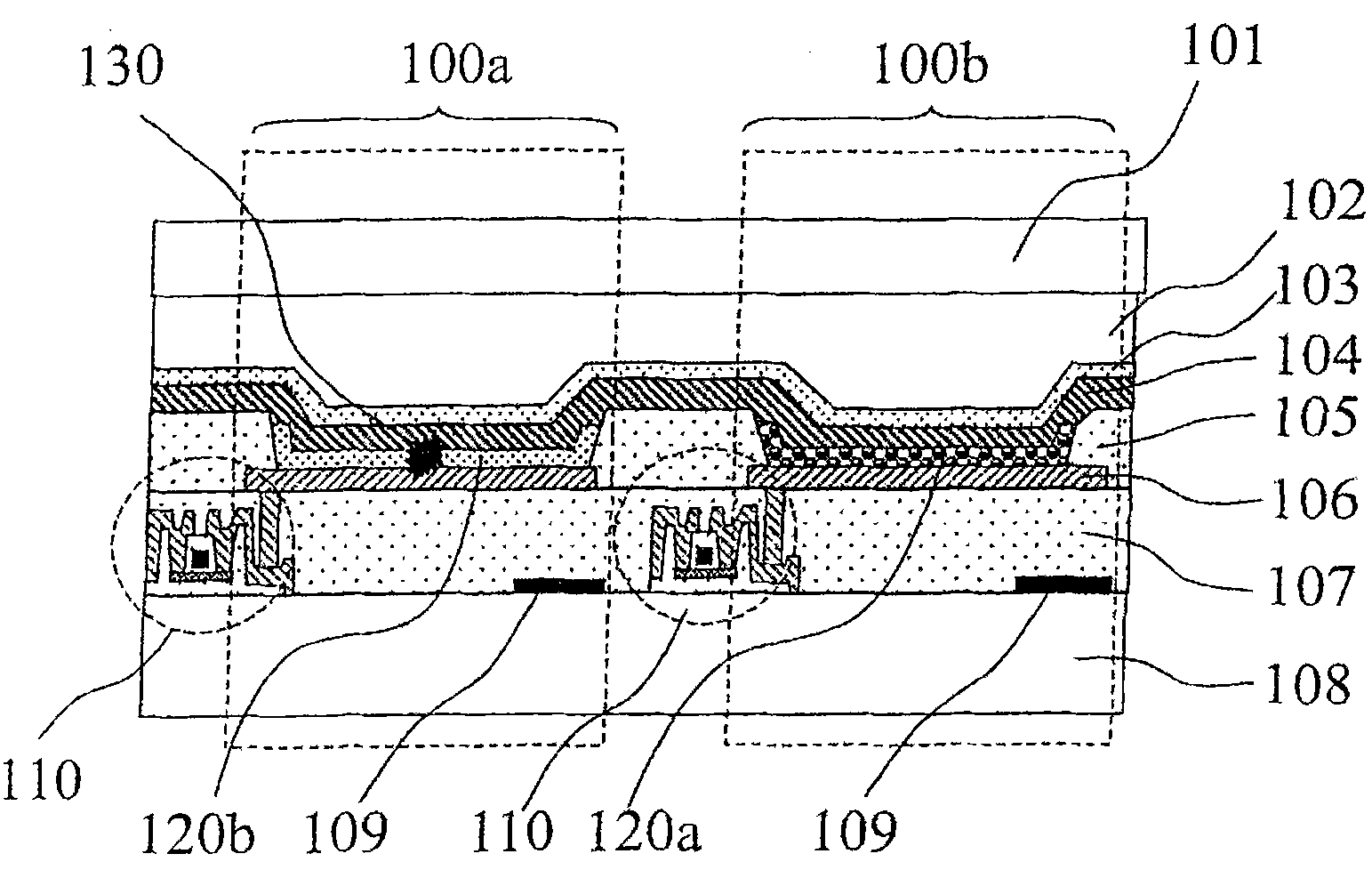
[0142] Figure 9 It is a plan view of a main substrate on which dedicated wiring for power supply to pixels and electrode pads are formed according to an embodiment of the present invention. In the backplane process, when manufacturing the main substrate 320 on which the TFTs and wiring are made, in order to be able to supply power together in units of the main substrate, the electrode pads 305 for power supply to the gate portion and the power supply wiring for the gate portion are simultaneously fabricated on both sides of the substrate. Wire 306 , electrode pad 307 for source portion power supply, source portion power supply wiring 308 , EL element second electrode power supply pad 309 , EL element second electrode power supply wiring 310 . At the same time, other wiring required for panel lighting is produced. In addition, in the present embodiment, a structure in which power is supplied from both sides of the main substrate is adopted, but a structure in which power is s...

Embodiment 2

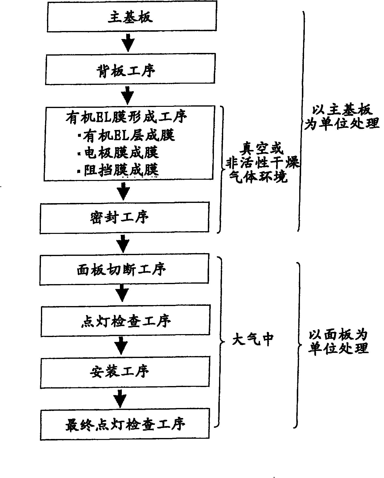
[0159] Figure 16 An example of the manufacturing process of the active-type organic EL panel when the lighting inspection and correction device according to the embodiment of the present invention is used is shown. with in figure 1 In the conventional process shown, the lighting inspection process is processed in units of panels, since the lighting inspection process can be performed in units of main substrates that have not undergone the sealing process, so it is easy to automate. In addition, regardless of the sealing structure of the panel , can take in the correction process that can correct pixel defects, so the yield rate of the panel with the resin sealing structure required in the large panel can be improved.

[0160] Figure 17 An example of the configuration of an organic EL display manufacturing system according to an embodiment of the present invention is shown. Here, an example in which the organic EL film forming process is performed by a vacuum film forming ...

Embodiment 3

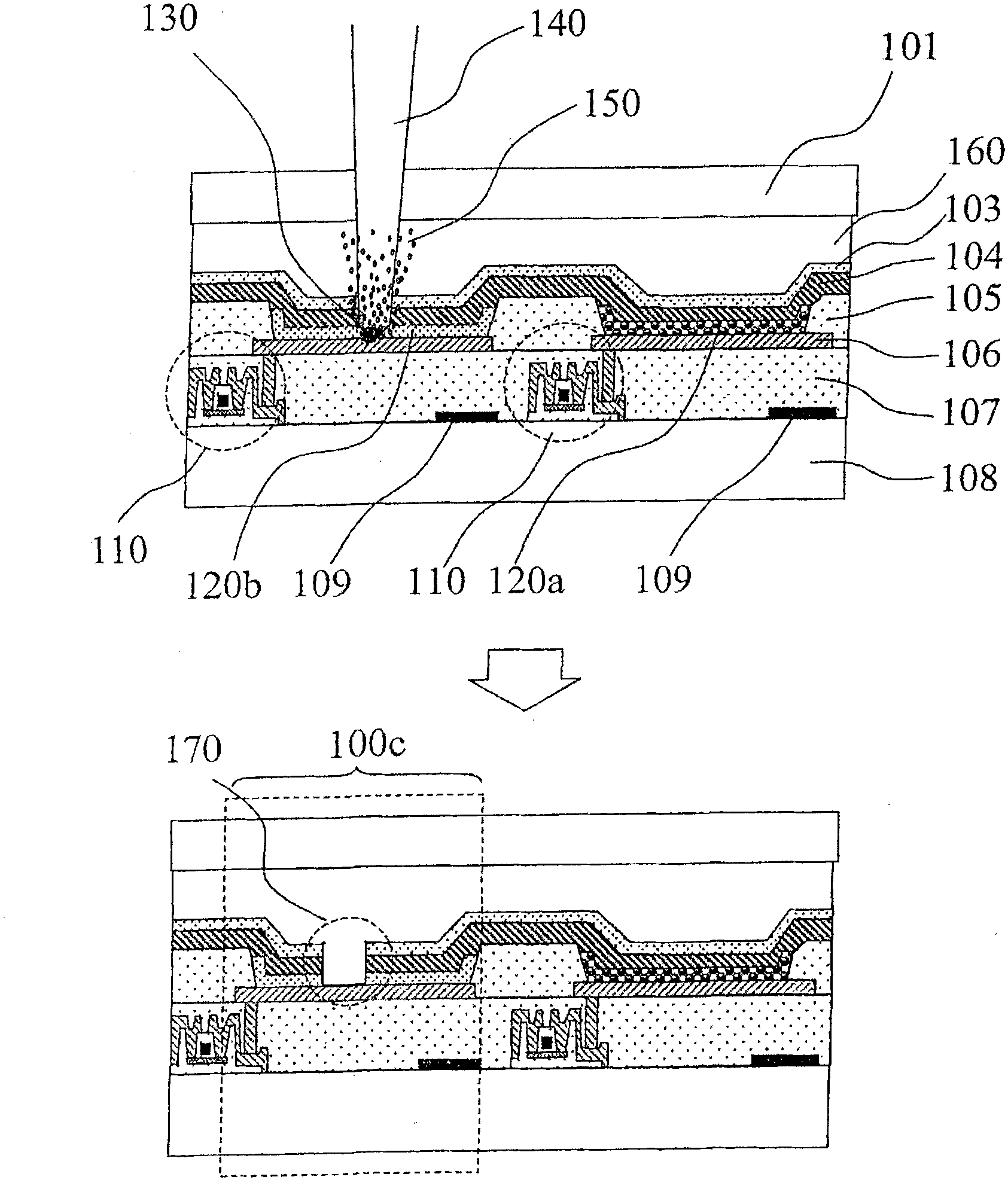
[0164] In order to ensure the light-emitting life of the organic EL panel, in the inspection and correction equipment according to the embodiment of the present invention, the dew point is managed below -70°C by inert dry gas such as dry nitrogen. In order to easily manage the dew point and save the inert dry gas, It is desirable to minimize the space within the inspection and correction equipment. Since the inspection and correction device of this embodiment is an optical device, it uses a frame structure with a glass plate as a window, and by arranging the detection system and laser irradiation system outside the glass plate, it is possible to greatly reduce the consumption of the inert dry gas. space.

[0165] Figure 18 An example of a lighting inspection device that lowers the space 801 filled with inert dry gas is shown. The stage 805, the main substrate 320, and the probe 802 of the lighting inspection device 806 are connected to the transfer chamber 804, and are loca...


PUM


Abstract

The invention provides a lighting inspection device of an organic EL display substrate and a method thereof. Even the final panel form is a resin sealing structure, the pixel defect can be restored, and the reliability of pixel after defect restoration is high, or the processing time of restoration inspection is short, or the success rate of defect restoration is high, and automation can be achieved and the productivity is high. Power is supplied to a special wiring of lighting inspection enabling each pixel of the organic EL element to light and to a special electrode pad, thereby each pixel is lighted. Based on the lighting result, defective pixels unlighted among all pixels and their positions are measured. When the foreign matter of the defect pixels is irradiated for defect restoration before sealing, a photomask having light-penetrating patterns enabling laser to pass through irradiates the positions of the defect based on the position information and size of the defect.

Description

technical field [0001] The present invention relates to an organic EL display substrate lighting inspection device, a lighting inspection method, and an organic EL display substrate defect inspection that perform automatic detection and selection of display defects of an organic EL panel and automatic correction of dark spots (defects) in units of main substrates Correction device and defect inspection and correction method, organic EL display panel correction equipment and correction method, organic EL display manufacturing system and manufacturing method. Background technique [0002] Compared with liquid crystal panels, organic EL (display) panels have a wider range of colors, higher brightness, faster response, and wider viewing angles. In addition to handling these excellent display performances, low power consumption is easy to achieve thinner, so in mobile phones, DSC (multiple Functional digital cameras), PMP (portable multimedia players) and other small panel fields...

Claims


Application Information

Patent Timeline
Patent Type & Authority Applications(China)
IPC IPC(8): G01N21/88G01B11/00H01L27/32H01L51/56
CPCH01L2924/0002H01L2924/00H05B33/10H10K71/00
Inventor 片冈文雄松浦宏育吉武康裕
Owner HITACHI HIGH-TECH CORP
Why Eureka
Try Eureka