
Novel optimized 150 W loading piece with aluminum nitride ceramic substrate
A technology of aluminum nitride ceramics and aluminum nitride substrates, which is applied in waveguide devices, electrical components, circuits, etc., can solve problems such as communication system design limitations, achieve good VSWR performance, increase area, and optimize design effects
- Summary
- Abstract
- Description
- Claims
- Application Information
AI Technical Summary
Problems solved by technology
Method used
Image

Examples
Embodiment Construction
[0013] Preferred embodiments of the present invention will be described in detail below in conjunction with the accompanying drawings.
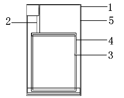
[0014] like figure 1 As shown, the new optimized version of the aluminum nitride ceramic substrate 150 watt load sheet includes a 5.7*9.55*1mm aluminum nitride substrate 1, the back of the aluminum nitride substrate 1 is printed with a back guide layer, and the front of the aluminum nitride substrate is printed There are wires 2 and resistors 3. The resistors 3 are connected by wires 2 to form a load circuit. The ground terminal of the load circuit is connected to the back conductor layer through the terminal ground silver paste, so that the load circuit can be grounded to form a loop. A protective glass film 4 is printed on the resistor 3, and a black protective film 5 is also printed on the upper surfaces of the conductive wire 2 and the protective glass film 4, so that the conductive wire 2, the resistor 3 and the protective glass film 4 c...
PUM
 Abstract
Description
Claims
Application Information