display device

A technology of a display device and a display area, which is applied in the directions of printing image acquisition, instruments, and calculation, can solve the problems of high cost and complex structure of the display device, and achieve the effect of simple structure and process.

Active Publication Date: 2019-12-20
INTERFACE OPTOELECTRONICS SHENZHEN +1
View PDF6 Cites 0 Cited by
  • Summary
  • Abstract
  • Description
  • Claims
  • Application Information

AI Technical Summary

Problems solved by technology

It can be seen that the structure of the display device is more complicated and the cost is higher

Method used


Image

  • display device
  • display device
  • display device

Examples


Embodiment Construction

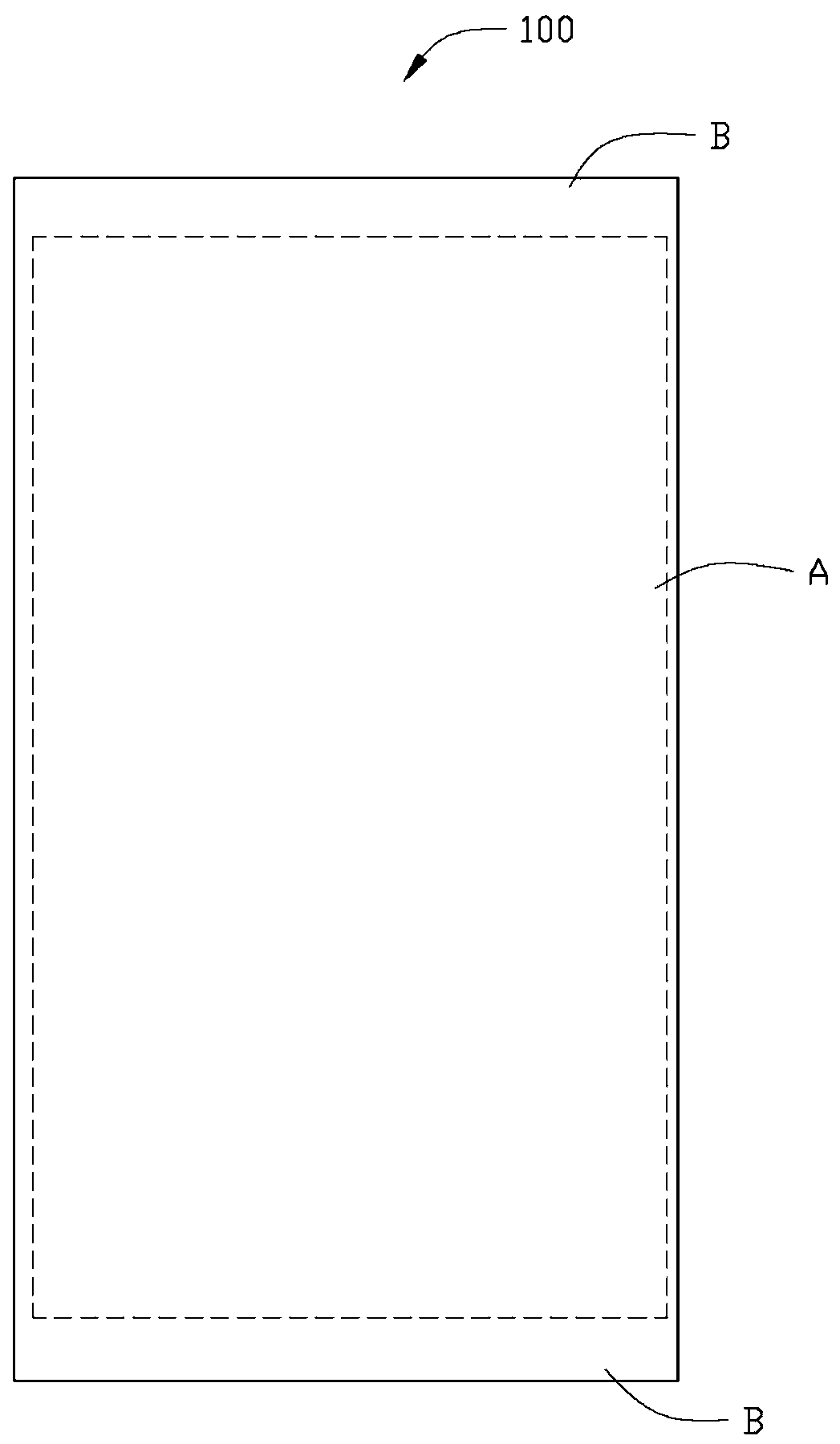
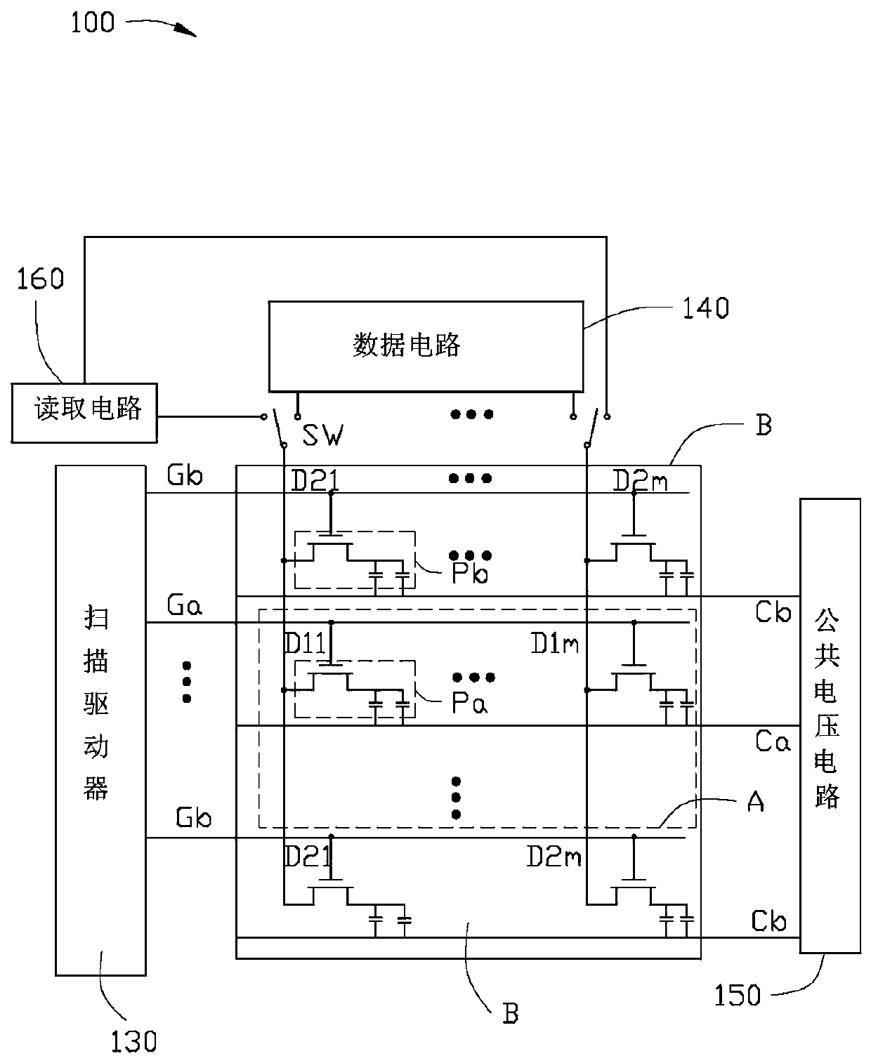
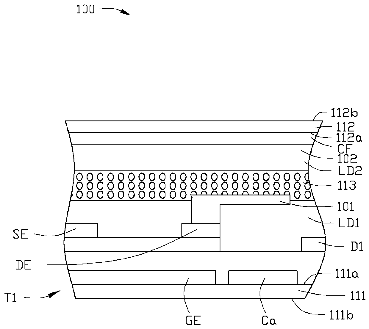
[0022] Please also refer to Figure 1-4 , figure 1 is a schematic plan view of the display device 100 according to the first embodiment of the present invention, figure 2 for figure 1 A block diagram of a display device 100 is shown, image 3 for figure 1 A schematic diagram of the (Pixel Unit) structure of one of the display pixel units in the display area of ​​the display device shown, Figure 4 for figure 1 A schematic structural diagram of one of the dummy pixel units (Dummy Pixel Unit) in the non-display area of ​​the display device shown. It should be noted that the hierarchical structure and electrode pattern of the dummy pixel unit described in this embodiment are the same as those of the display pixel unit, the only difference being that the dummy pixel unit is not used for displaying images.

[0023] see figure 1 , the display device 100 includes a display area A and a non-display area B, and the non-display area B is located on opposite sides of the display ...


PUM


Abstract

A display device includes a first substrate, a second substrate, a display medium and a fingerprint recognition module sandwiched between the first and second substrates. The areas of the first and second substrates corresponding to the display medium are defined as a display area and a non-display area. Corresponding to the non-display area, a data extension line and first and second auxiliary electrodes are arranged between the first and second substrates. The fingerprint identification module is arranged in the non-display area, including an ultrasonic transmitting unit and an ultrasonic receiving element. The ultrasonic emitting unit is arranged on the first or second substrate for emitting ultrasonic waves. The ultrasonic receiving element is arranged between the first and second substrates, and is used to receive the ultrasonic wave and convert the ultrasonic wave into a fingerprint identification signal and transmit it to the first auxiliary electrode. The data extension line reads the fingerprint identification signal from the first auxiliary electrode to Identify fingerprints.

Description

technical field [0001] The invention relates to a display device, in particular to a display device which has a display function and realizes fingerprint identification by using ultrasonic waves. Background technique [0002] In the existing fingerprint recognition display device, the display module used for image display and the fingerprint recognition module are set independently. It usually includes a sound wave sending unit, a sound wave receiving unit and an array of switching elements for detecting object characteristics (such as fingerprints). It can be seen that the structure of the display device is relatively complicated and the cost is relatively high. Contents of the invention [0003] In view of this, it is necessary to provide a display device with image display and fingerprint recognition functions with a relatively simple structure. [0004] A display device, comprising a first substrate, a second substrate opposite to the first substrate, and a display m...

Claims


Application Information

Patent Timeline
Patent Type & Authority Patents(China)
IPC IPC(8): G06K9/00
CPCG06V40/1306G02F1/13338
Inventor 陈俊吉黄上育陈祯佑王世育
Owner INTERFACE OPTOELECTRONICS SHENZHEN
Why Eureka
Try Eureka