Pixel compensation circuit used for active organic light-emitting diode display

A technology of light emitting diodes and compensation circuits, applied in the field of pixel compensation circuits, can solve the problems of insufficient layout area, process variation, leakage and the like

Inactive Publication Date: 2016-04-20
AU OPTRONICS CORP
View PDF0 Cites 8 Cited by
  • Summary
  • Abstract
  • Description
  • Claims
  • Application Information

AI Technical Summary

Problems solved by technology

[0004] However, when the AMOLED panel is going to be developed to high resolution, the insufficient layout area will become a problem due to the smaller and smaller pixel size.
At the same time, in the c

Method used


Image

  • Pixel compensation circuit used for active organic light-emitting diode display
  • Pixel compensation circuit used for active organic light-emitting diode display
  • Pixel compensation circuit used for active organic light-emitting diode display

Examples


Embodiment Construction

[0039] In order to make the technical content disclosed in this application more detailed and complete, reference may be made to the drawings and the following various specific embodiments of the present invention, and the same symbols in the drawings represent the same or similar components. However, those skilled in the art should understand that the examples provided below are not intended to limit the scope of the present invention. In addition, the drawings are only for schematic illustration and are not drawn according to their original scale.

[0040] The specific implementation manners of various aspects of the present invention will be further described in detail below with reference to the accompanying drawings.

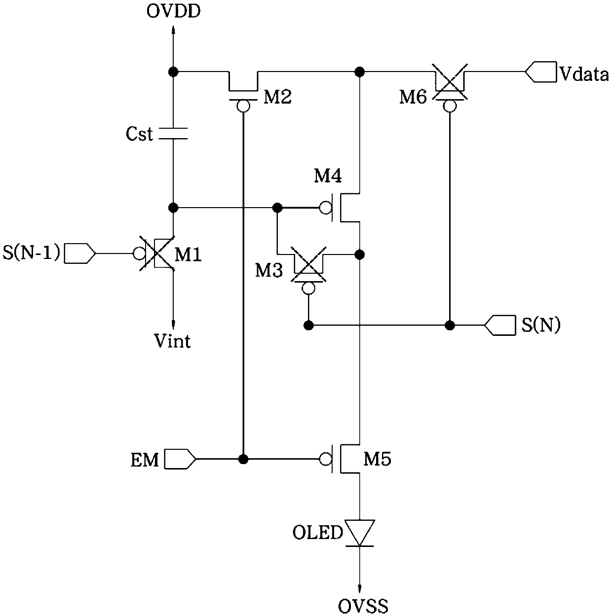
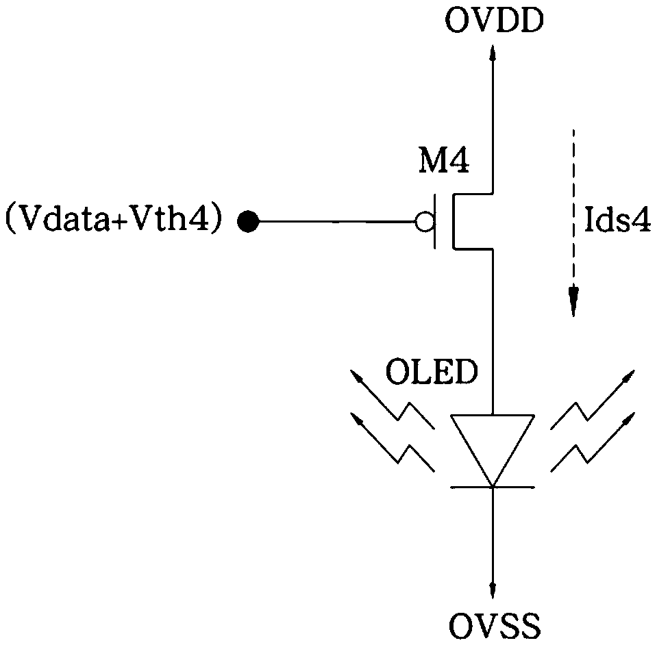
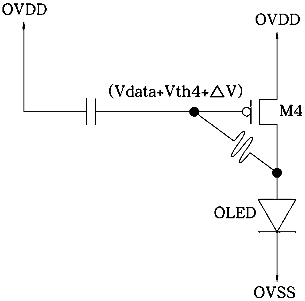
[0041] figure 1 A schematic structural diagram of a pixel compensation circuit for an active organic light emitting diode display in the prior art is shown. Figure 2A show figure 1 A schematic diagram of the gate drive voltage applied to the fourth swit...


PUM


Abstract

The invention provides a pixel compensation circuit used for an active organic light-emitting diode display. The pixel compensation circuit comprises a first switch, a second switch, a third switch, a fourth switch, a fifth switch, a sixth switch, a seventh switch and an organic light-emitting diode, wherein the control end of the first switch receives drive signals of the (N-1)-level grid electrode; the control end of the second switch receives an ignition control signal; the control end of the third switch receives drive signals of the N-level grid electrode; the control end of the fourth switch is electrically coupled to the first end of the first switch; the second end of the fifth switch is electrically coupled to the second end of the third switch; the control end of the sixth switch receives ignition control signals; the control end of the seventh switch receives drive signals of the N-level grid electrode; the anode of the organic light-emitting diode is coupled to the second end of the sixth switch, and the cathode of the organic light-emitting diode is coupled to a second voltage. Compared with the prior art, the fourth switch and the fifth switch form a bigrid framework, and the second end of the fifth switch is electrically coupled to the second end of the third switch, so that the situation of electricity leakage between a source electrode and the drain electrode of the third switch can be prevented, and a poor dimly bright point generated in a low gray-scale image is improved.

Description

technical field [0001] The invention relates to an active organic light emitting diode (ActiveMatrixOrganicLightEmittingDiode, AMOLED) display, in particular to a pixel compensation circuit of the AMOLED display. Background technique [0002] In recent years, conventional displays have been gradually replaced by portable thin flat panel displays. Self-illuminating displays such as organic or inorganic light emitting displays have more advantages than other flat panel displays because organic or inorganic light emitting displays can provide a wide viewing angle, good contrast ratio, and have a fast response speed. In this way, organic or inorganic light-emitting displays have attracted widespread attention as next-generation displays, especially organic light-emitting diode (Organic Light Emitting Diode, OLED) displays that include a light-emitting layer formed by organic materials, while providing color images, compared with inorganic light-emitting displays. It has higher ...

Claims


Application Information

Patent Timeline
IPC IPC(8): G09G3/3233
CPCG09G3/3233G09G2320/0214
Inventor 邱治文蔡轩名
Owner AU OPTRONICS CORP
Why Eureka
Try Eureka