A display device and method of making the same

A display device and electrode layer technology, which is applied in semiconductor/solid-state device manufacturing, semiconductor devices, electrical components, etc., can solve problems such as the second electrode is easy to break, increase device brightness and light extraction efficiency, reduce cost, and reduce device resistance. Reduced effect

Active Publication Date: 2018-11-13
KUNSHAN GO VISIONOX OPTO ELECTRONICS CO LTD
View PDF6 Cites 7 Cited by
  • Summary
  • Abstract
  • Description
  • Claims
  • Application Information

AI Technical Summary

Problems solved by technology

[0005] The technical problem to be solved by the present invention lies in the problems that the second electrode of the existing display device is easy to break, so as to provide a display, which adopts a double-layer conductive film layer structure, which effectively reduces the undulation height of the second electrode to ensure that the OLED cathode The structure of the film layer is flattened, thus effectively avoiding the problem of fracture of the second electrode layer

Method used


Image

  • A display device and method of making the same
  • A display device and method of making the same
  • A display device and method of making the same

Examples


Embodiment Construction

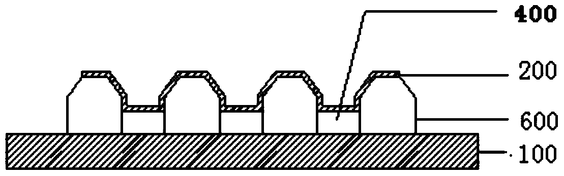
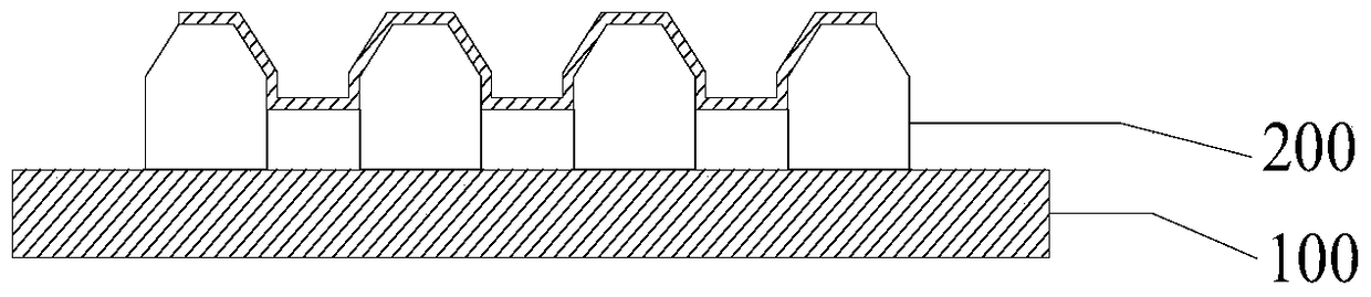
[0027] In order to make the object, technical solution and advantages of the present invention clearer, the implementation manner of the present invention will be further described in detail below in conjunction with the accompanying drawings.

[0028] This invention may be embodied in many different forms and should not be construed as limited to the embodiments set forth herein. Rather, these embodiments are provided so that this disclosure will be thorough and complete and will fully convey the concept of the invention to those skilled in the art, and the present invention will only be defined by the appended claims. In the drawings, the size and relative sizes of layers and regions may be exaggerated for clarity. It will be understood that when an element such as a layer, region or substrate is referred to as being "formed on" or "disposed on" another element, it can be directly on the other element or present middle element. In contrast, when an element is referred to a...


PUM


Abstract

The invention relates to the display device. The display device comprises a first electrode layer arranged on a substrate, multiple pixel limitation layers, and an organic luminescent layer and a second electrode layer which are formed between the pixel limitation layers, wherein the pixel limitation layers comprises a first pixel limitation layer and a second pixel limitation layer, a conduction film layer is formed between the first pixel limitation layer and the second pixel limitation layer, and the second electrode layer is electrically communicated with the conduction film layer. The display device employs a double-layer conduction film layer structure, fluctuation height of the second electrode can be effectively reduced to guarantee flattening of an OLED cathode film layer structure, and a fracture problem of the second electrode layer can be effectively avoided.

Description

technical field [0001] The invention relates to a display device, and also relates to a preparation method of the display device. Background technique [0002] Organic light-emitting devices (English full name organic lighting emitting display, referred to as OLED) have the advantages of active light emission, wide color gamut, fast response, wide viewing angle, high contrast ratio, planarization, etc., and are the development trend of the next generation of display and lighting technology. [0003] An organic light-emitting display device includes an anode layer, a light-emitting layer, and a cathode layer. The cathode layer in an OLED device is currently made through a Common Metal Mask (common metal mask). In addition, due to the influence of the height of the pixel definition layer (Pillar layer), the cathode layer The film layer presents a continuous ups and downs state; in the process of lamination and practical application, there may be bad phenomena such as fracture ...

Claims


Application Information

Patent Timeline
Patent Type & Authority Patents(China)
IPC IPC(8): H01L27/32H01L51/56H01L51/52H01L51/54
Inventor 曹朝干
Owner KUNSHAN GO VISIONOX OPTO ELECTRONICS CO LTD
Why Eureka
Try Eureka