Rapid epitaxial wafer exposure device

A technology of exposure device and epitaxial wafer, which is applied in the direction of printing device, optics, printing equipment, etc., to achieve the effects of convenient operation, prolonging service life, and improving the degree of braking and intelligence

Inactive Publication Date: 2017-05-10
DIMENSION TECH
View PDF0 Cites 0 Cited by
  • Summary
  • Abstract
  • Description
  • Claims
  • Application Information

AI Technical Summary

Problems solved by technology

However, general imaging devices cannot realize this principle, and a special fast epitaxial wafer exposure device is needed to perform better exposure and photography, so as to make real images and prevent problems before they happen

Method used


Image

  • Rapid epitaxial wafer exposure device

Examples


Embodiment Construction

[0018] The present invention is described in further detail now in conjunction with accompanying drawing. These drawings are all simplified schematic diagrams, which only illustrate the basic structure of the present invention in a schematic manner, so they only show the configurations related to the present invention.

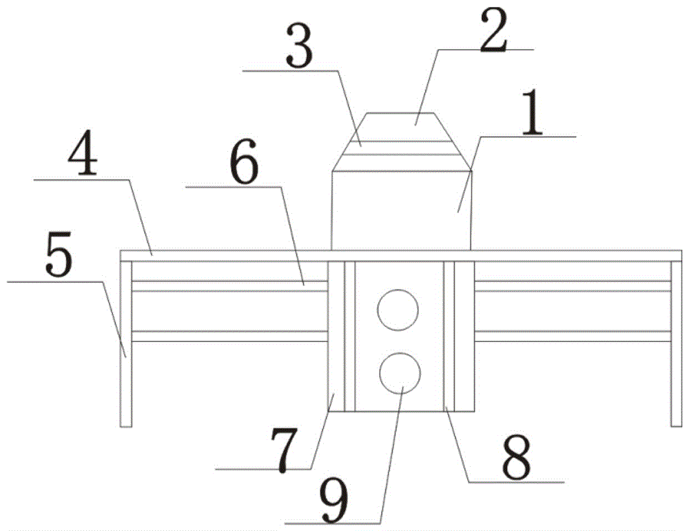
[0019] Such as figure 1 The preferred embodiment of the rapid epitaxial wafer exposure device of the present invention shown includes an image aligner 1, and a digital electronic polarized picture capture structure 2 is arranged on the top of the image aligner 1, and between the digital electronic polarized picture capture structure 2 and the image aligner 1 An exposure lamp 3 is installed, and the digital electronic polarization frame capture structure 2 is connected to the image aligner 1 through an adjustable device. The bottom of the image aligner 1 is located on an operating platform 4, and the image aligner 1 and the operating platform 4 are hinged. The...


PUM


Abstract

The invention discloses a rapid epitaxial wafer exposure device comprising an image locating device. The top part of the image locating device is provided with a digital electronic polarization frame capture structure. An exposure lamp is installed between the digital electronic polarization frame capture structure and the image locating device. The digital electronic polarization frame capture structure and the image locating device are connected through an adjustable device. The bottom part of the image locating device is arranged on an operating platform. The image locating device and the operating platform are hinged. Holders are installed on the position close to the lower surface of the two side surfaces of the operating platform. The holders and the operating platform are fixedly connected. Energy consumption plates are connected between the two holders. There are more than one energy consumption plates which are provided with guide rails. According to the rapid epitaxial wafer exposure device, the braking and intelligent degree of equipment can be enhanced so that the safety coefficient can be greatly enhanced, the exposure accuracy can be enhanced, the line is enabled to be more uniform and the service life of the exposure equipment can also be prolonged, and thus the device has great adjustment performance, simple debugging and convenient operation.

Description

technical field [0001] The invention relates to an imaging device, in particular to a fast epitaxial wafer exposure device. Background technique [0002] In the era of rapid information development, people have found in a large number of social activities that they are engaged in that only relying on original materials and documents as the only original archives to preserve and provide various utilization services can no longer meet the current needs. Social groups, individuals and all parties need to collect and obtain some powerful original materials. These original materials are indispensable legal documents in social activities, information resources for various activities and learning, and these information resources can be captured by microfilm. method, and then make a copy of the original, the image information on the microform is a real record of the original, and can truly reproduce the information content of the original document, which is a very advanced preservat...

Claims


Application Information

Patent Timeline
Patent Type & Authority Applications(China)
IPC IPC(8): G03B27/54G03B27/52
CPCG03B27/54G03B27/52
Inventor 姚海林
Owner DIMENSION TECH
Why Eureka
Try Eureka